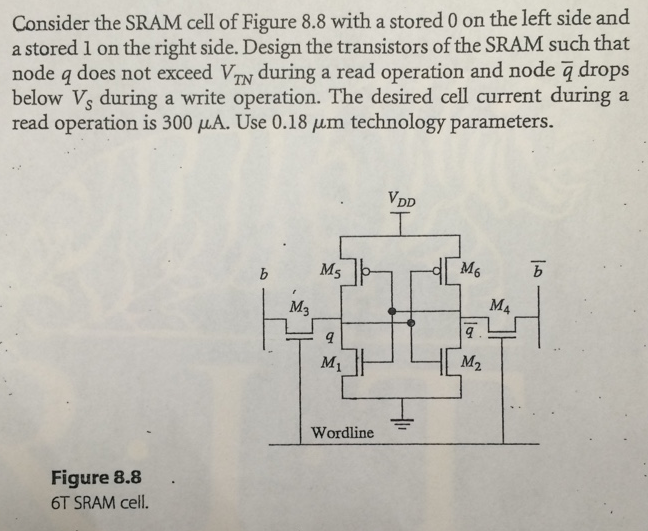
Consider the SRAM cell of Figure 8.8 with a stored 0 on the left side and a stored 1 on the right side. Design the transistors of the SRAM such that node q does not exceed VTN during a read operation and node q¯ drops below VS during a write operation. The desired cell current during a read operation is 300 μA. Use 0.18 μm technology parameters. Figure 8.8 6 ST SRAM cell.
