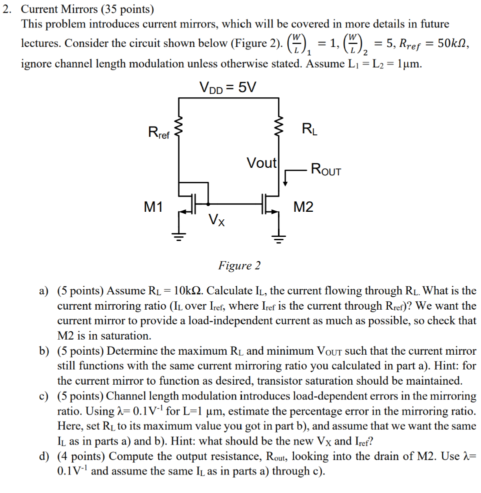
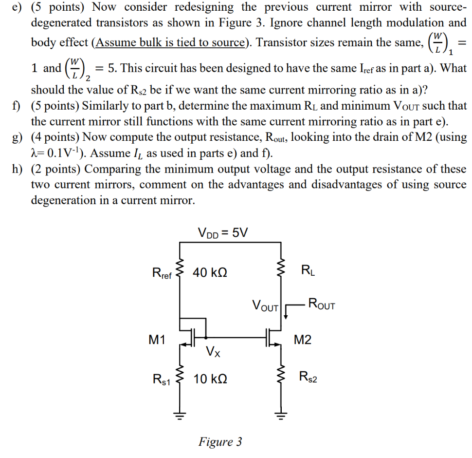
Current Mirrors (35 points) This problem introduces current mirrors, which will be covered in more details in future lectures. Consider the circuit shown below (Figure 2). (W/L)1 = 1, (W/L)2 = 5, Rref = 50 kΩ, ignore channel length modulation unless otherwise stated. Assume L1 = L2 = 1 μm. Figure 2 a) (5 points) Assume RL = 10 kΩ. Calculate IL, the current flowing through RL. What is the current mirroring ratio ( IL over Iref , where Iref is the current through Rref )? We want the current mirror to provide a load-independent current as much as possible, so check that M2 is in saturation. b) (5 points) Determine the maximum RL and minimum VOut such that the current mirror still functions with the same current mirroring ratio you calculated in part a). Hint: for the current mirror to function as desired, transistor saturation should be maintained. c) (5 points) Channel length modulation introduces load-dependent errors in the mirroring ratio. Using λ = 0.1 V−1 for L = 1 μm, estimate the percentage error in the mirroring ratio. Here, set RL to its maximum value you got in part b ), and assume that we want the same IL as in parts a) and b). Hint: what should be the new VX and Iref ? d) (4 points) Compute the output resistance, Rout, , looking into the drain of M2. Use λ = 0.1 V−1 and assume the same IL as in parts a) through c). e) (5 points) Now consider redesigning the previous current mirror with source-degenerated transistors as shown in Figure 3. Ignore channel length modulation and body effect ( Assume bulk is tied to source). Transistor sizes remain the same, (WL)1 = 1 and (WL)2 = 5. This circuit has been designed to have the same Iref as in part a). What should the value of Rs2 be if we want the same current mirroring ratio as in a)? f) (5 points) Similarly to part b, determine the maximum RL and minimum VOut such that the current mirror still functions with the same current mirroring ratio as in part e). g) (4 points) Now compute the output resistance, Rout , looking into the drain of M2 (using λ = 0.1 V−1 ). Assume IL as used in parts e) and f ). h) (2 points) Comparing the minimum output voltage and the output resistance of these two current mirrors, comment on the advantages and disadvantages of using source degeneration in a current mirror. Figure 3