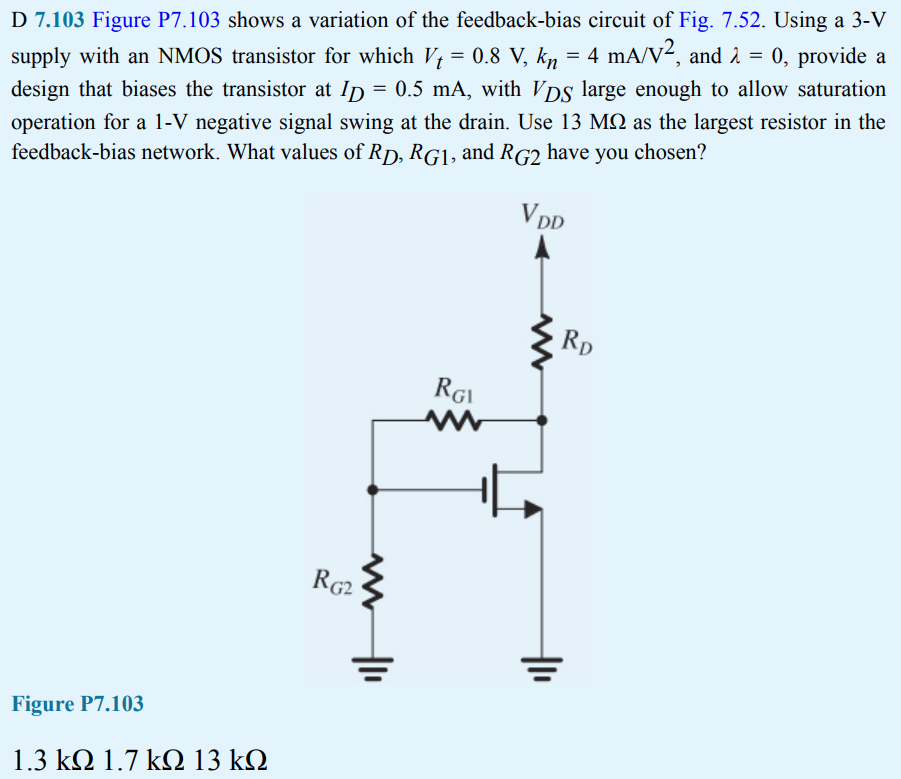
D 7.103 Figure P7.103 shows a variation of the feedback-bias circuit of Fig. 7.52. Using a 3-V supply with an NMOS transistor for which Vt = 0.8 V, kn = 4 mA/V2, and λ = 0, provide a design that biases the transistor at ID = 0.5 mA, with VDS large enough to allow saturation operation for a 1-V negative signal swing at the drain. Use 13 MΩ as the largest resistor in the feedback-bias network. What values of RD, RG1, and RG2 have you chosen?

You'll get a detailed, step-by-step and expert verified solution.
 Work With Experts to Reach at Correct Answers