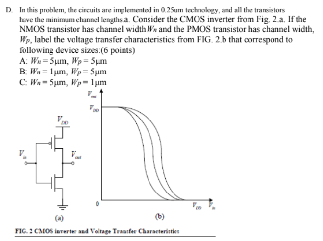
D. In this problem, the circuits are implemented in 0.25 um technology, and all the transistors have the minimum channel lengths. a. Consider the CMOS inverter from Fig.2. a. If the NMOS transistor has channel width Wn and the PMOS transistor has channel width, Wp, label the voltage transfer characteristics from FIG.2. b that correspond to following device sizes:(6 points) A: Wn = 5 μm, Wp = 5 μm B: Wn = 1 μm, Wp = 5 μm C:Wn = 5 μm, Wp = 1 μm (a) (b) FIG.2 CMOS inverter and Voltage Transfer Characteristics
D. In this problem, the circuits are implemented in 0.25 um technology, and all the transistors have the minimum channel lengths. a. Consider the CMOS inverter from Fig.2. a. If the NMOS transistor has channel width Wn and the PMOS transistor has channel width, Wp, label the voltage transfer characteristics from FIG.2. b that correspond to following device sizes:(6 points) A: Wn = 5 μm, Wp = 5 μm B: Wn = 1 μm, Wp = 5 μm C:Wn = 5 μm, Wp = 1 μm (a) (b) FIG.2 CMOS inverter and Voltage Transfer Characteristics

Image text
D. In this problem, the circuits are implemented in 0.25 um technology, and all the transistors have the minimum channel lengths.a. Consider the CMOS inverter from Fig. 2.a. If the NMOS transistor has channel width W n and the PMOS transistor has channel width, W p , label the voltage transfer characteristics from FIG. 2.b that correspond to following device sizes:(6 points) A: W n = 5 μ m , W p = 5 μ m B: W n = 1 μ m , W p = 5 μ m C : W n = 5 μ m , W p = 1 μ m (a) (b) FIG. 2 CMOS inverter and Voltage Transfer Characteristics

Detailed Answer