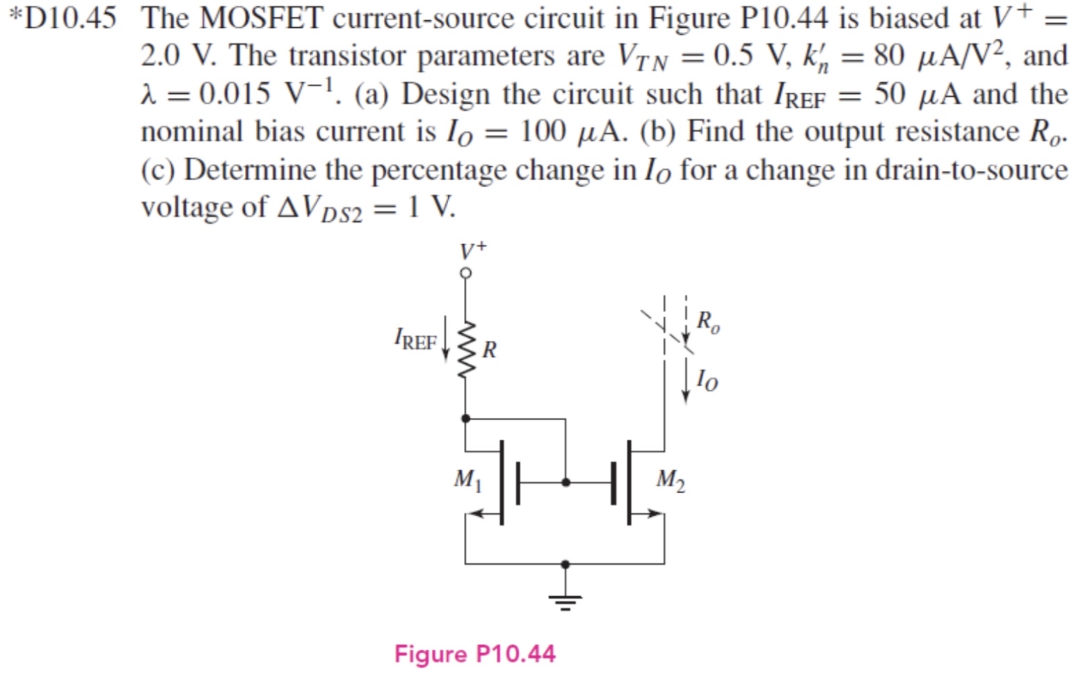
*D10.45 The MOSFET current-source circuit in Figure P10.44 is biased at V+ = 2.0 V. The transistor parameters are VTN = 0.5 V, kn′ = 80 μA/V2, and λ = 0.015 V −1. (a) Design the circuit such that IREF = 50 μA and the nominal bias current is IO = 100 μA. (b) Find the output resistance Ro. (c) Determine the percentage change in IO for a change in drain-to-source voltage of ΔVDS2 = 1 V. Figure P10.44

*D10.45 The MOSFET current-source circuit in Figure P10.44 is biased at V+ = 2.0 V. The transistor parameters are VTN = 0.5 V, kn′ = 80 μA/V2, and λ = 0.015 V −1. (a) Design the circuit such that IREF = 50 μA and the nominal bias current is IO = 100 μA. (b) Find the output resistance Ro. (c) Determine the percentage change in IO for a change in drain-to-source voltage of ΔVDS2 = 1 V. Figure P10.44

Image text
*D10.45 The MOSFET current-source circuit in Figure P10.44 is biased at V + = 2.0 V . The transistor parameters are V T N = 0.5 V , k n = 80 μ A / V 2 , and λ = 0.015 V 1 . (a) Design the circuit such that I R E F = 50 μ A and the nominal bias current is I O = 100 μ A . (b) Find the output resistance R o . (c) Determine the percentage change in I O for a change in drain-to-source voltage of Δ V D S 2 = 1 V . Figure P10.44

Detailed Answer

Answer
  • Student Reviews:
  • (2)
  • Correct answers (2)
  • Complete solution (2)
  • Step-by-step solution (2)
  • Fully explained (2)