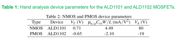
Design a 2-input CMOS Schmitt NOR gate (Draw the designed circuit and show all MOSFET sizes) that satisfies the following requirements: Input down trip voltage is equal to 2/3 VDD and input up trip is equal to 1/3 VDD Minimum input gate capacitance for each input Output drive strength is equal to a symmetrical inverter with WN/LN = 4 μm/2 μm The design should yield a reasonable propagation delay Use channel lengths of 2 μm for all MOSFETs. Assume KN′ = 40 μA/V2, KP′ = 16 μA/V2, VTN = 1 V, VTP = −1 V, and VDD = 5 V.