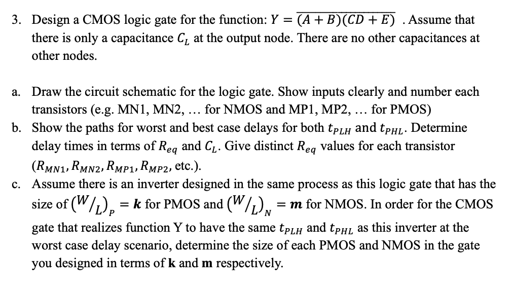
Design a CMOS logic gate for the function: Y = (A + B)(CD + E ). Assume that there is only a capacitance CL at the output node. There are no other capacitances at other nodes. a. Draw the circuit schematic for the logic gate. Show inputs clearly and number each transistors (e.g. MN1, MN2, ... for NMOS and MP1, MP2, .. for PMOS) b. Show the paths for worst and best case delays for both tPLH and tPHL. Determine delay times in terms of Req and CL. Give distinct Req values for each transistor (RMN1, RMN2, RMP1, RMP2, etc.). c. Assume there is an inverter designed in the same process as this logic gate that has the size of (W/L)P = k for PMOS and (W/L)N = m for NMOS. In order for the CMOS gate that realizes function Y to have the same tPLH and tPHL as this inverter at the worst case delay scenario, determine the size of each PMOS and NMOS in the gate you designed in terms of k and m respectively.
Design a CMOS logic gate for the function: Y = (A + B)(CD + E ). Assume that there is only a capacitance CL at the output node. There are no other capacitances at other nodes. a. Draw the circuit schematic for the logic gate. Show inputs clearly and number each transistors (e.g. MN1, MN2, ... for NMOS and MP1, MP2, .. for PMOS) b. Show the paths for worst and best case delays for both tPLH and tPHL. Determine delay times in terms of Req and CL. Give distinct Req values for each transistor (RMN1, RMN2, RMP1, RMP2, etc.). c. Assume there is an inverter designed in the same process as this logic gate that has the size of (W/L)P = k for PMOS and (W/L)N = m for NMOS. In order for the CMOS gate that realizes function Y to have the same tPLH and tPHL as this inverter at the worst case delay scenario, determine the size of each PMOS and NMOS in the gate you designed in terms of k and m respectively.

Image text
  1. Design a CMOS logic gate for the function: Y = ( A + B ) ( C D + E ) ¯ . Assume that there is only a capacitance C L at the output node. There are no other capacitances at other nodes. a. Draw the circuit schematic for the logic gate. Show inputs clearly and number each transistors (e.g. MN1, MN2, ... for NMOS and MP1, MP2, .. for PMOS) b. Show the paths for worst and best case delays for both t P L H and t P H L . Determine delay times in terms of R e q and C L . Give distinct R e q values for each transistor ( R M N 1 , R M N 2 , R M P 1 , R M P 2 , etc.). c. Assume there is an inverter designed in the same process as this logic gate that has the size of ( W / L L = k for PMOS and ( W / L ) N = m for NMOS. In order for the CMOS gate that realizes function Y to have the same t P L H and t P H L as this inverter at the worst case delay scenario, determine the size of each PMOS and NMOS in the gate you designed in terms of k and m respectively.

Detailed Answer