Design of a CMOS inverter circuit: Use the same device parameters as in Problem 5.6. The power supply voltage is VDD = 3.3 V. The channel length of both transistors is Ln = Lp = 0.8 um. (a) Determine the (Wn/Wp) ratio so that the switching (inversion) threshold voltage of the circuit is Vth = 1.4 V. (b) The CMOS fabrication process used to manufacture this inverter allows a variation of the VT0,n value by
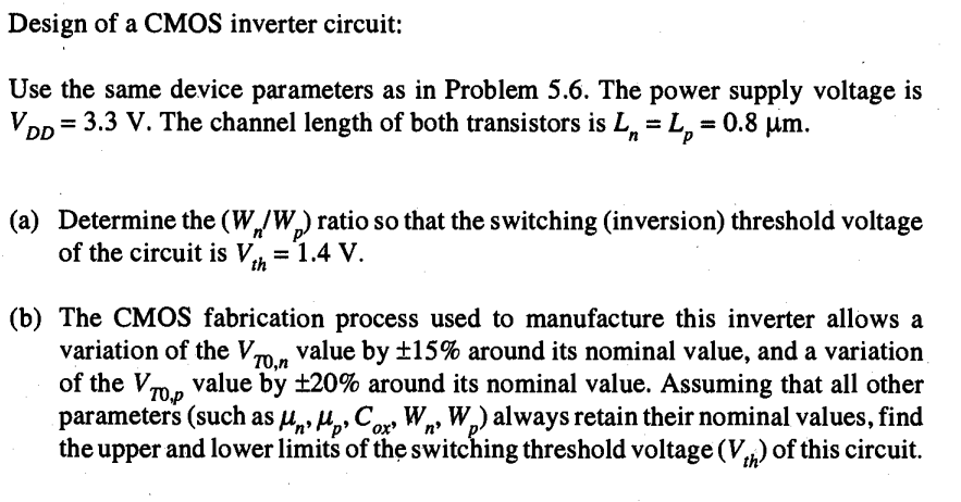
Design of a CMOS inverter circuit: Use the same device parameters as in Problem 5.6. The power supply voltage is VDD = 3.3 V. The channel length of both transistors is Ln = Lp = 0.8 um. 
(a) Determine the (Wn/Wp) ratio so that the switching (inversion) threshold voltage of the circuit is Vth = 1.4 V. 
(b) The CMOS fabrication process used to manufacture this inverter allows a variation of the VT0,n value by

Image text
Design of a CMOS inverter circuit: Use the same device parameters as in Problem 5.6. The power supply voltage is VDD = 3.3 V. The channel length of both transistors is Ln = Lp = 0.8 um. (a) Determine the (Wn/Wp) ratio so that the switching (inversion) threshold voltage of the circuit is Vth = 1.4 V. (b) The CMOS fabrication process used to manufacture this inverter allows a variation of the VT0,n value by

Detailed Answer

Answer
  • Student Reviews:
  • (3)
  • Correct answers (2)
  • Complete solution (2)
  • Step-by-step solution (2)
  • Fully explained (2)