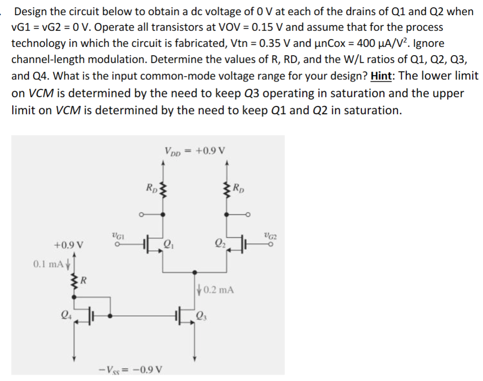
Design the circuit below to obtain a dc voltage of 0 V at each of the drains of Q1 and Q2 when vG1 = vG2 = 0 V. Operate all transistors at VOV = 0.15 V and assume that for the process technology in which the circuit is fabricated, Vtn = 0.35 V and μnCox = 400 μA/V2. Ignore channel-length modulation. Determine the values of R, RD, and the W/L ratios of Q1, Q2, Q3, and Q4. What is the input common-mode voltage range for your design? Hint: The lower limit on VCM is determined by the need to keep Q3 operating in saturation and the upper limit on VCM is determined by the need to keep Q1 and Q2 in saturation.