Design the CS stage for a voltage gain (Av = Vout/Vin) of -4, a power budget (P) of 2 mW, and a voltage drop of 200 mV across Rs. The overdrive voltage of M1 must not exceed 300 mV, and R1+R2 must consume less than 0.1 mW. Use μnCox = 200 μA/V2, VTH = 0.4 V, λ = 0, VDD = 1.8 V and. The coupling capacitors (C) are short circuits at frequencies of interest. (a) Determine Rs1, R1, R2 (b) Determine W/L (c) Determine RD (d) Verify that M1 operates in saturation. If not, why is it?
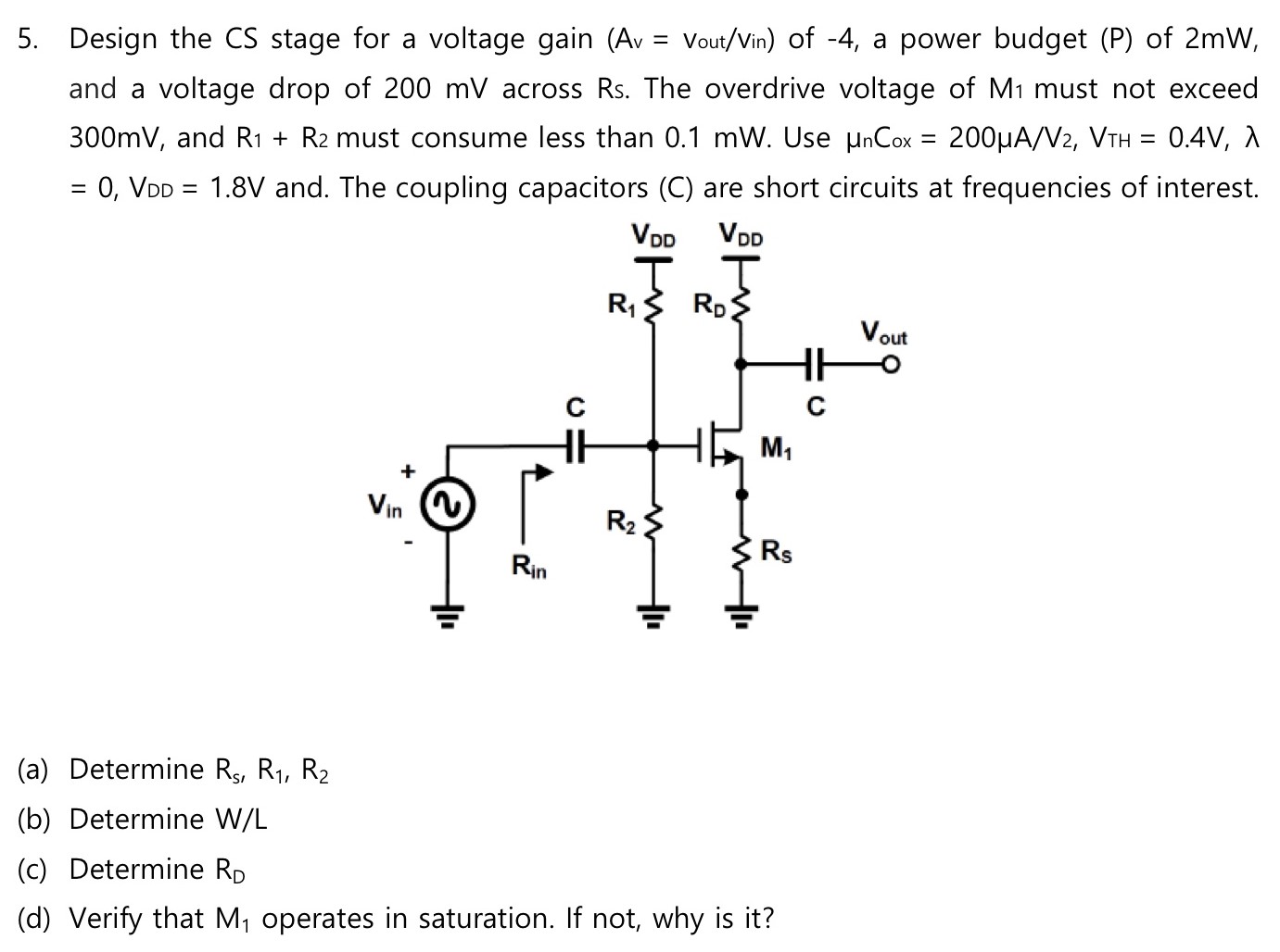
Design the CS stage for a voltage gain (Av = Vout/Vin) of -4, a power budget (P) of 2 mW, and a voltage drop of 200 mV across Rs. The overdrive voltage of M1 must not exceed 300 mV, and R1+R2 must consume less than 0.1 mW. Use μnCox = 200 μA/V2, VTH = 0.4 V, λ = 0, VDD = 1.8 V and. The coupling capacitors (C) are short circuits at frequencies of interest. (a) Determine Rs1, R1, R2 (b) Determine W/L (c) Determine RD (d) Verify that M1 operates in saturation. If not, why is it?

Image text
  1. Design the CS stage for a voltage gain ( A v = Vout / Vin ) of -4 , a power budget ( P ) of 2 mW , and a voltage drop of 200 mV across Rs. The overdrive voltage of M 1 must not exceed 300 mV , and R 1 + R 2 must consume less than 0.1 mW . Use μ n C ox = 200 μ A / V 2 , V TH = 0.4 V , λ = 0 , V D D = 1.8 V and. The coupling capacitors ( C ) are short circuits at frequencies of interest. (a) Determine R s 1 , R 1 , R 2 (b) Determine W / L (c) Determine R D (d) Verify that M 1 operates in saturation. If not, why is it?

Detailed Answer