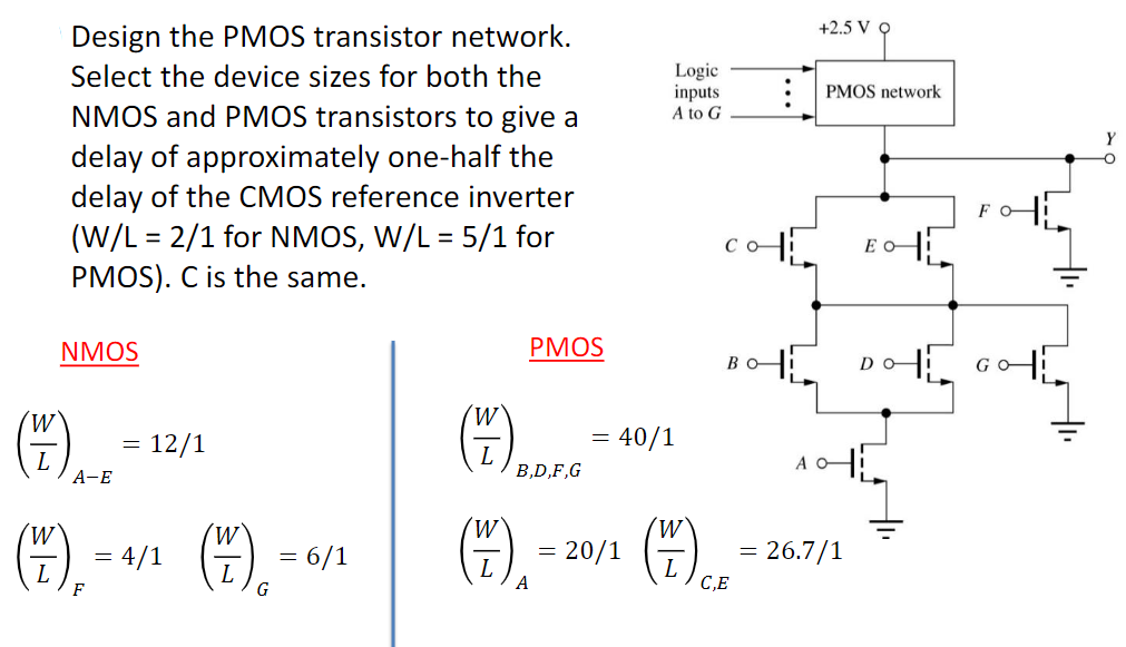
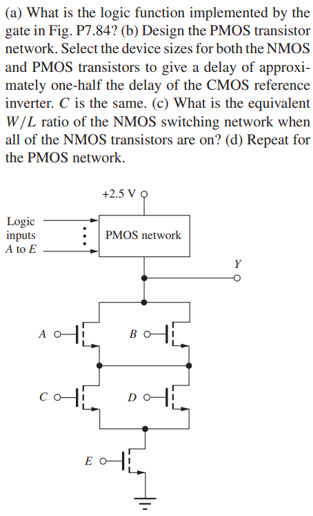
Design the PMOS transistor network. Select the device sizes for both the NMOS and PMOS transistors to give a delay of approximately one-half the delay of the CMOS reference inverter (W/L=2/1 for NMOS, W/L=5/1 for PMOS). C is the same.
Image text
Design the PMOS transistor network. Select the device sizes for both the NMOS and PMOS transistors to give a delay of approximately one-half the delay of the CMOS reference inverter (W/L=2/1 for NMOS, W/L=5/1 for PMOS). C is the same.