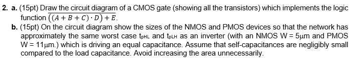
Draw the circuit diagram of a CMOS gate (showing all the transistors) which implements the logic function ((A + B + C) • D) + E b. (15pt) On the circuit diagram show the sizes of the NMOS and PMOS devices so that the network has approximately the same worst case tpHL and tpLH as an inverter (with an NMOS W = 5µm and PMOS W = 11µm.) which is driving an equal capacitance. Assume that self-capacitances are negligibly small compared to the load capacitance. Avoid increasing the area unnecessarily.