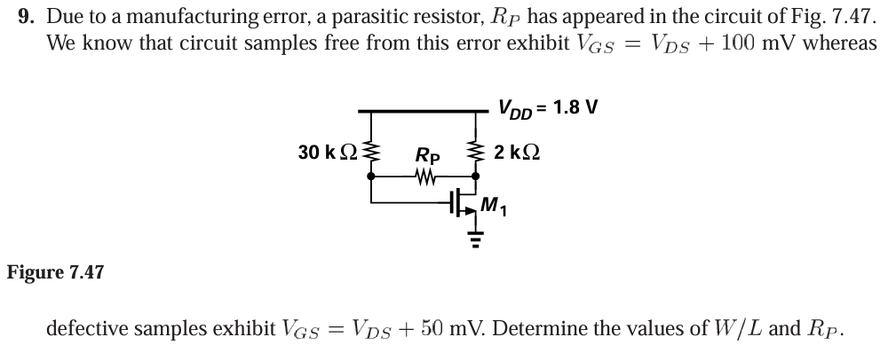
Due to a manufacturing error, a parasitic resistor, RP has appeared in the circuit of Fig. 7.47. We know that circuit samples free from this error exhibit VGS = VDS + 100 mV whereas defective samples exhibit VGS = VDS+50 mV. Determine the values of W/L and RP. Figure 7.47
Due to a manufacturing error, a parasitic resistor, RP has appeared in the circuit of Fig. 7.47. We know that circuit samples free from this error exhibit VGS = VDS + 100 mV whereas defective samples exhibit VGS = VDS+50 mV. Determine the values of W/L and RP. Figure 7.47

Image text
  1. Due to a manufacturing error, a parasitic resistor, R P has appeared in the circuit of Fig. 7.47. We know that circuit samples free from this error exhibit V G S = V D S + 100 mV whereas
Figure 7.47 defective samples exhibit V G S = V D S + 50 mV . Determine the values of W / L and R P .

Detailed Answer