Enhancement-mode NMOS and PMOS devices both have parameters L = 4 µm and tox = 500 A0 . For the NMOS transistor, VT N = 0.6 V, µn = 675 cm2/V - s, and the channel width is Wn for the PMOS transistor, VTP = -0.6 V, µP = 375 cm2/V -s, and the channel width is WP. Design the widths of the two transistors such that they are electrically equivalent and the drain current in the PMOS transistor is ID = 0.8 mA when it is biased in the saturation region at VSG = 5 V. What are the values of Kn, KP, Wn, and WP?
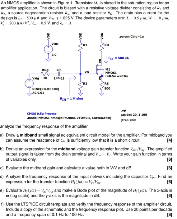
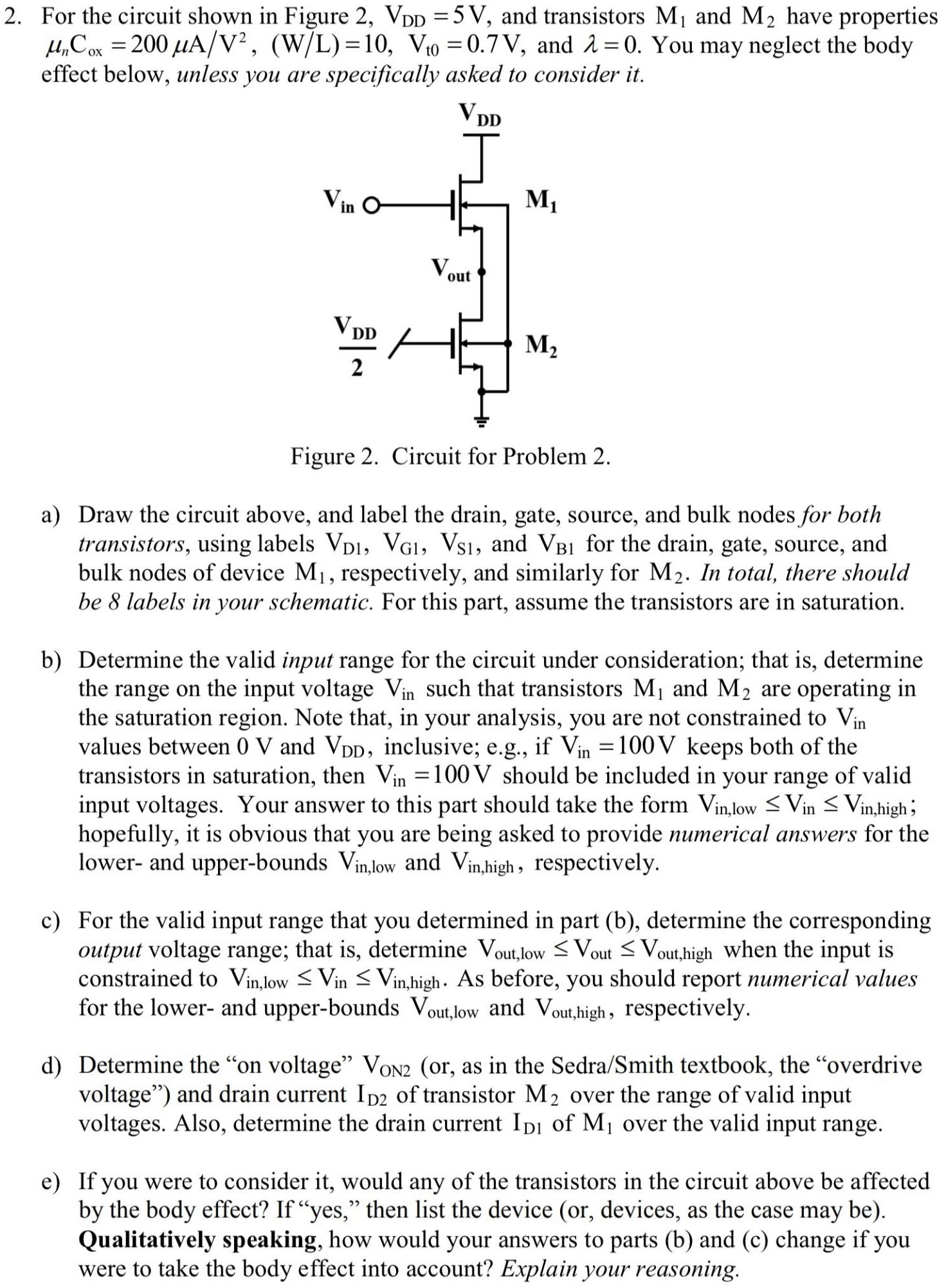
Image text
Enhancement-mode NMOS and PMOS devices both have parameters L = 4 µm and tox = 500 A0 . For the NMOS transistor, VT N = 0.6 V, µn = 675 cm2/V - s, and the channel width is Wn for the PMOS transistor, VTP = -0.6 V, µP = 375 cm2/V -s, and the channel width is WP. Design the widths of the two transistors such that they are electrically equivalent and the drain current in the PMOS transistor is ID = 0.8 mA when it is biased in the saturation region at VSG = 5 V. What are the values of Kn, KP, Wn, and WP?