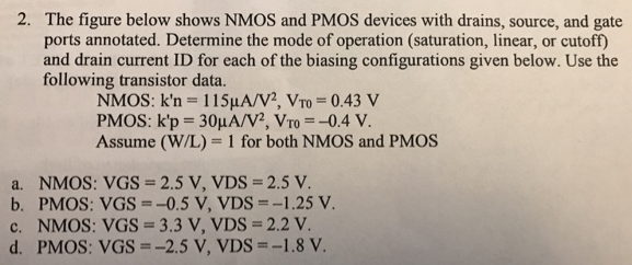
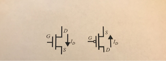
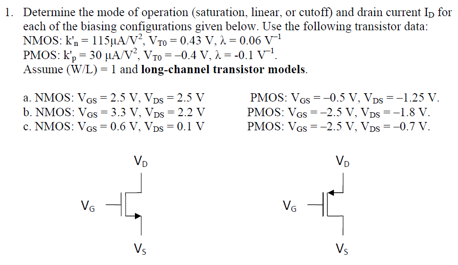
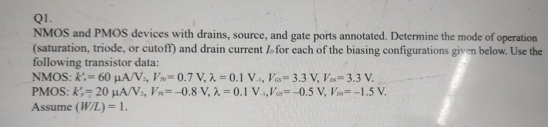
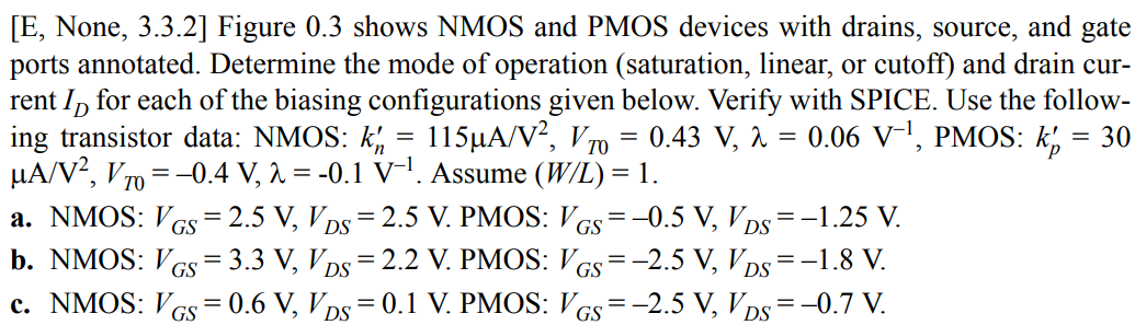
Figure 0.3 shows NMOS and PMOS devices with drains, source, and gate ports annotated. Determine the mode of operation (saturation, linear, or cutoff) and drain current ID for each of the biasing configurations given below. Verify with SPICE. Use the following transistor data: NMOS: k’n = 115 µA/V2 , VT0 = 0.43 V, λ = 0.06 V–1, PMOS: k’p = 30 µA/V2 , VT0 = –0.4 V, λ = -0.1 V–1. Assume (W/L) = 1. a. NMOS: VGS = 2.5 V, VDS = 2.5 V. PMOS: VGS = –0.5 V, VDS = –1.25 V. b. NMOS: VGS = 3.3 V, VDS = 2.2 V. PMOS: VGS = –2.5 V, VDS = –1.8 V. c. NMOS: VGS = 0.6 V, VDS = 0.1 V. PMOS: VGS = –2.5 V, VDS = –0.7 V

You'll get a detailed, step-by-step and expert verified solution.
 Work With Experts to Reach at Correct Answers