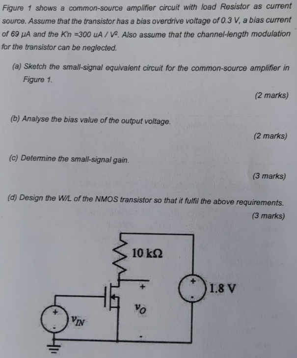
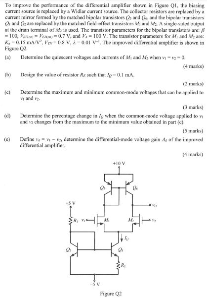
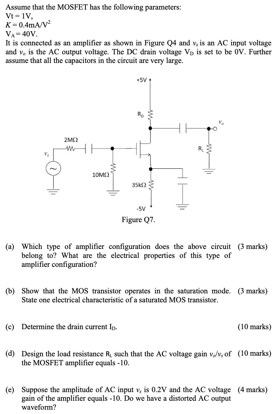
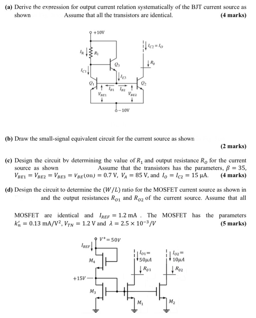
Figure 1 shows a common-source amplifier circuit with load Resistor as current source. Assume that the transistor has a bias overdrive voltage of 0.3 V, a bias current of 69 μA and the Kn = 300 A/V2. Also assume that the channel-length modulation for the transistor can be neglected. (a) Sketch the small-signal equivalent circuit for the common-source amplifier in Figure 1. (2 marks) (b) Analyse the bias value of the output voltage. (2 marks) (c) Determine the small-signal gain. (3 marks) (d) Design the W/L of the NMOS transistor so that it fulfil the above requirements. (3 marks)