D 8.42 The circuit in Fig. 8.15(a) is fabricated in the 0.18-μm CMOS process whose parameters are specified in Table K.1 (Appendix K). VDD = 1.8 V. Design the circuit to obtain a voltage gain Av = -20 V/V. Use devices of equal length L operating at I = 100 μA and |Vov| = 0.2 V. Determine the required values of VG, L, (W/L)1, and (W/L)2.
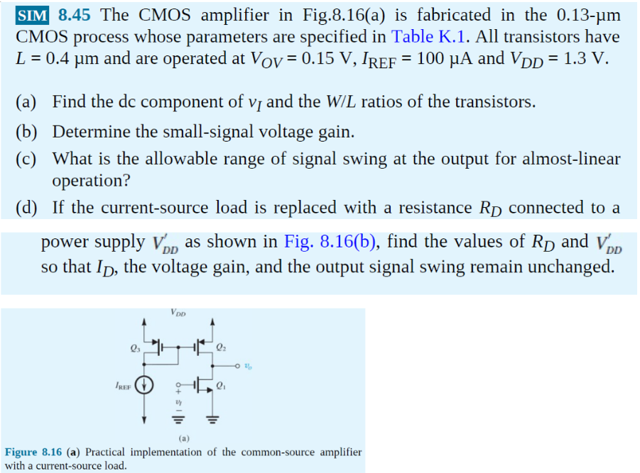
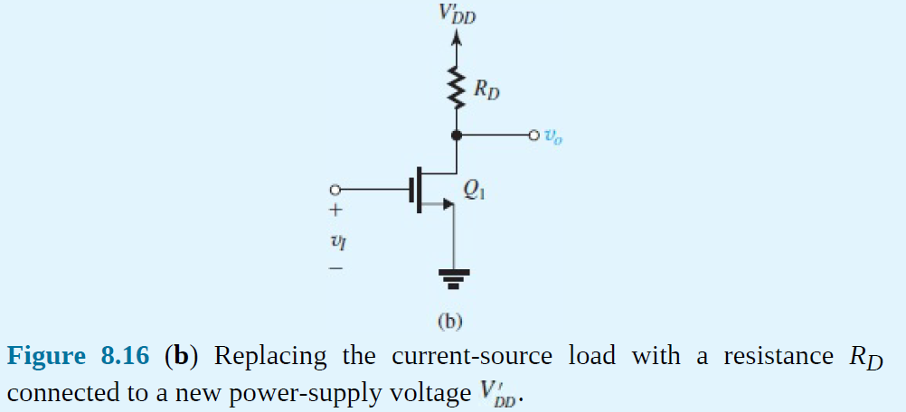
Image text
D 8.42 The circuit in Fig. 8.15(a) is fabricated in the 0.18-μm CMOS process whose parameters are specified in Table K.1 (Appendix K). VDD = 1.8 V. Design the circuit to obtain a voltage gain Av = -20 V/V. Use devices of equal length L operating at I = 100 μA and |Vov| = 0.2 V. Determine the required values of VG, L, (W/L)1, and (W/L)2.


![(20 points) The cascode current source shown below utilizes two identical PMOS transistors with VDD = 1.8 V, Vtp = −0.5 V, VA′ = −6 V/μm, and μpCox = 100 μA/V2. Design the circuit to obtain I = 50 μA and Ro = 1 MΩ and to allow for the maximum possible voltage swing at the output terminal of the current source. Utilize |Vov| = 0.2 V. (a) Specify the required values of the dc bias voltages VG1 and VG2. [ 5 points] (b) What is the maximum allowable voltage at the output? [5 points] (c) Specify the values of W/L and L for Q1 and Q2. [10 points ]](https://www.doubtrix.com/uploads/editor/1105099255hFmBQkiFgj.jpg)