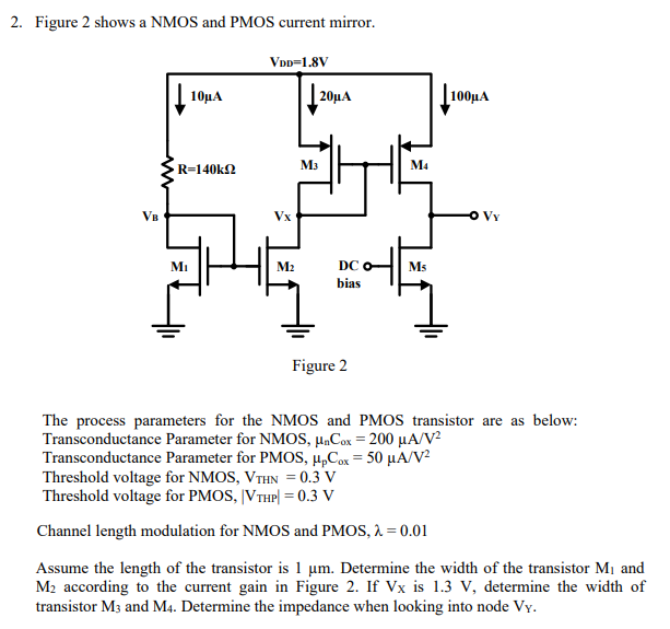
Figure 2 shows a NMOS and PMOS current mirror. Figure 2 The process parameters for the NMOS and PMOS transistor are as below: Transconductance Parameter for NMOS, μnCox = 200 μA/V2 Transconductance Parameter for PMOS, μpCox = 50 μA/V2 Threshold voltage for NMOS, VTHN = 0.3 V Threshold voltage for PMOS, |VTHP| = 0.3 V Channel length modulation for NMOS and PMOS, λ = 0.01 Assume the length of the transistor is 1 μm. Determine the width of the transistor M1 and M2 according to the current gain in Figure 2. If VX is 1.3 V, determine the width of transistor M3 and M4. Determine the impedance when looking into node VY.
