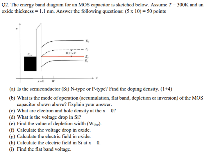
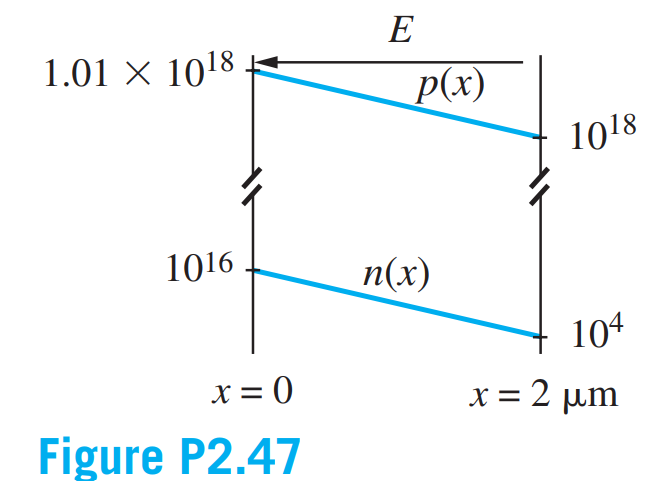
Figure P2.47 gives the electron and hole concentrations in a 2-µm-wide region of silicon. In addition, there is a constant electric field of 25 V/cm present in the sample. What is the total current density at x = 0? What are the individual drift and diffusion components of the hole and electron current densities at x = 1.0 µm? Assume that the electron and hole mobilities are 350 and 150 cm2/V•s, respectively.
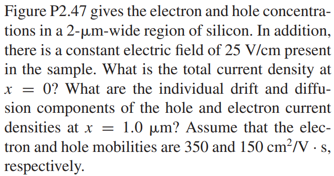
Drift and diffusion currents are the two mechanisms that contribute to the flow of charge carriers i.e. electrons and holes in semiconductors. The combination of these two mechanisms results in overall current flow within n-type or p-type semiconductor device.
Drift Current Density: When an electric field is applied across a semiconductor material, charge carriers (electrons or holes) tends to move in direction or opposite direction of electric field. Electrons move in the direction opposite to the electric field, while holes move in the direction of the electric field. The currents in semiconductor because of this movement of charge carriers is called as drift current. The drift current density is governed by Ohm's law for semiconductors and can be written as:
Diffusion current density: The diffusion current occurs in semiconductors due to difference in charge carrier concentration at different locations in the semiconductor material. The movement of charge carriers i.e. holes (in p-type semiconductors) or electrons (in n-type semiconductors) exists from higher concentration regions to lower concentration regions. The current flows in the semiconductor because of this concentration gradient and is known as the diffusion current. The diffusion current density can be written as:
Total current density is sum of both drift current density and diffusion current density.

You'll get a detailed, step-by-step and expert verified solution.
 Work With Experts to Reach at Correct Answers