Find the maximum allowable W/L for the access transistors Q5 and Q6 of the SRAM cell in the figure below, so that in a read operation, the voltage at Q and Q¯ do not change by more than |Vth|. Assume that the SRAM is fabricated in a 0.18−μm technology for which VDD = 1.8 V, Vtn = |Vtp| = 0.5 V and that (W/L)1 = (W/L)3 = 1.5. (20 points)
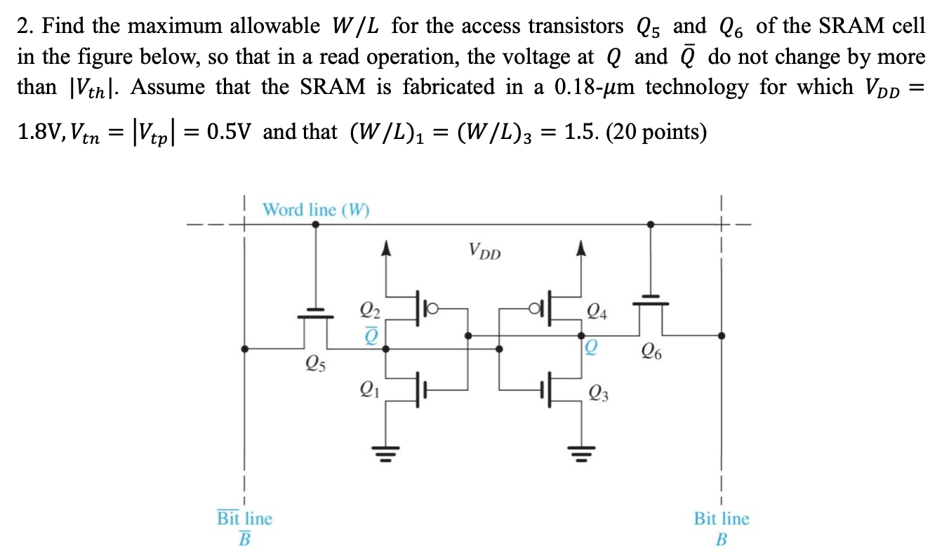
Find the maximum allowable W/L for the access transistors Q5 and Q6 of the SRAM cell in the figure below, so that in a read operation, the voltage at Q and Q¯ do not change by more than |Vth|. Assume that the SRAM is fabricated in a 0.18−μm technology for which VDD = 1.8 V, Vtn = |Vtp| = 0.5 V and that (W/L)1 = (W/L)3 = 1.5. (20 points)

Image text
  1. Find the maximum allowable W / L for the access transistors Q 5 and Q 6 of the SRAM cell in the figure below, so that in a read operation, the voltage at Q and Q ¯ do not change by more than | V t h | . Assume that the SRAM is fabricated in a 0.18 μ m technology for which V D D = 1.8 V , V t n = | V t p | = 0.5 V and that ( W / L ) 1 = ( W / L ) 3 = 1.5 . (20 points)

Detailed Answer