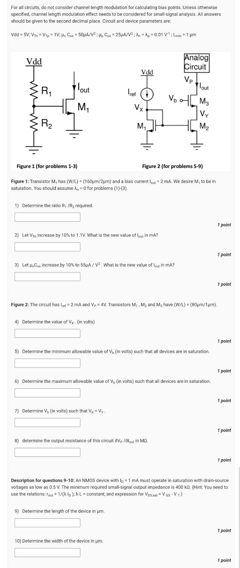
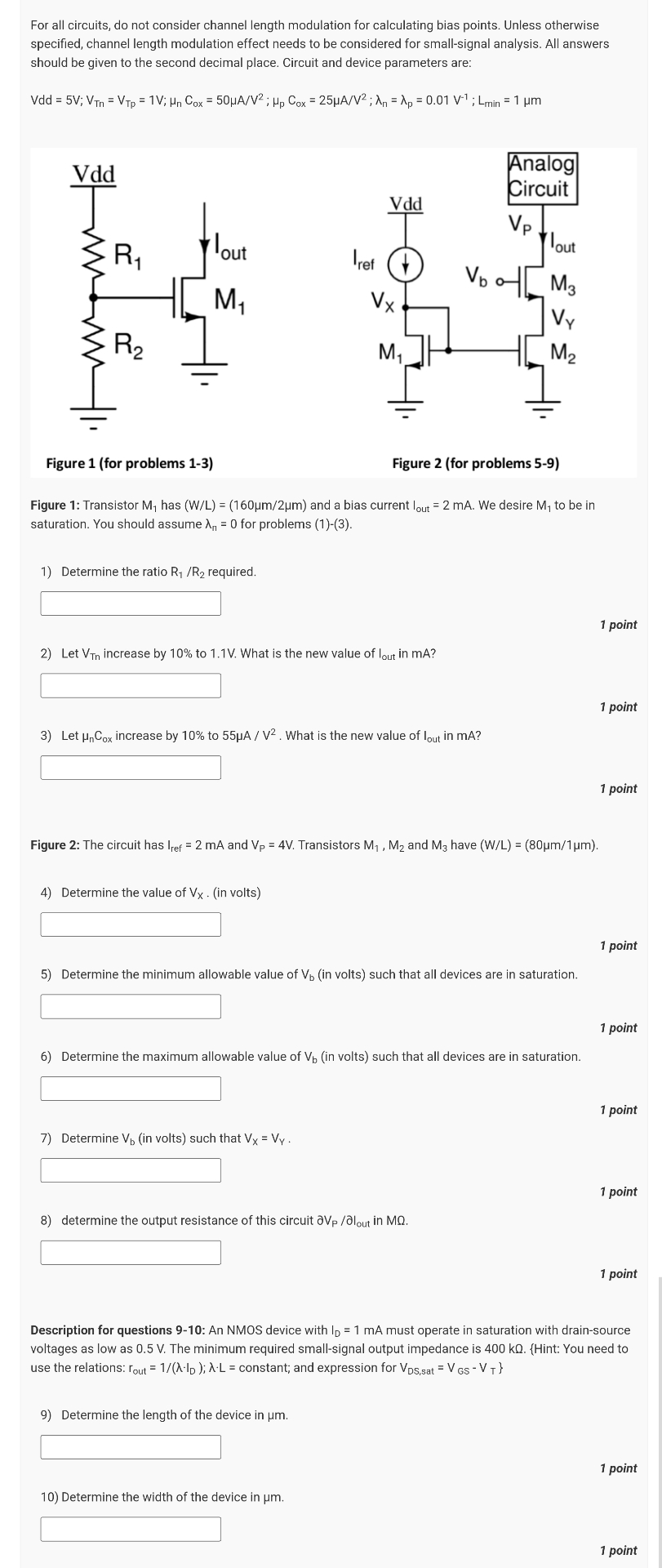
For all circuits, do not consider channel length modulation for calculating bias points. Unless otherwise specified, channel length modulation effect needs to be considered for small-signal analysis. All answers should be given to the second decimal place. Circuit and device parameters are: Vdd = 5 V; VTnn = VTp = 1 V; μnCox = 50 μA/V2; μpCox = 25 μA/V2; λn = λp = 0.01 V−1; Lmin = 1 μm Figure 1 (for problems 1-3) Figure 2 (for problems 5-9) Figure 1: Transistor M1 has (W/L) = (160 μm/2 μm) and a bias current Iout = 2 mA. We desire M1 to be in saturation. You should assume λn = 0 for problems (1)-(3). Determine the ratio R1 /R2 required. 1 point Let VTn increase by 10% to 1.1 V. What is the new value of Iout in mA ? 1 point Let μnCox increase by 10% to 55 μA/V2. What is the new value of Iout in mA ? 1 point Figure 2: The circuit has Iref = 2 mA and VP = 4 V. Transistors M1, M2 and M3 have (W/L) = (80 μm/1 μm). Determine the value of vx. (in volts) 1 point Determine the minimum allowable value of Vb (in volts) such that all devices are in saturation. 1 point Determine the maximum allowable value of Vb (in volts) such that all devices are in saturation. 1 point Determine Vb (in volts) such that VX = VY. 1 point determine the output resistance of this circuit ∂Vp/Iout in MQ. 1 point Description for questions 9-10: An NMOS device with ID = 1 mA must operate in saturation with drain-source voltages as low as 0.5 V. The minimum required small-signal output impedance is 400 kΩ. {Hint: You need to use the relations: rout = 1 /(λ⋅ID); λ⋅L = constant; and expression for VDS, sat = VGS−VT }Determine the length of the device in μm. 1 point Determine the width of the device in μm. 1 point