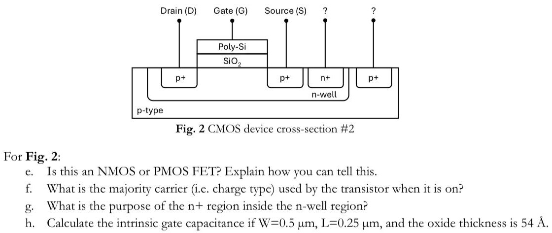
For Fig. 2: e. Is this an NMOS or PMOS FET? Explain how you can tell this. f. What is the majority carrier (i. e. charge type) used by the transistor when it is on? g. What is the purpose of the n+ region inside the n-well region? h. Calculate the intrinsic gate capacitance if W = 0.5 μm, L = 0.25 μm, and the oxide thickness is 54 Å. Fig. 2 CMOS device cross-section #2