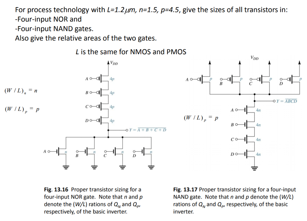
For process technology with L = 1.2 um, n = 1.5, p = 4.5, give the sizes of all transistors in: -Four-input NOR and -Four-input NAND gates. Also give the relative areas of the two gates. is the same for NMOS and PMOS Fig. 13.16 Proper transistor sizing for a four-input NOR gate. Note that n and p denote the (W/L) rations of QN and QP, respectively, of the basic inverter. Fig. 13.17 Proper transistor sizing for a four-input NAND gate. Note that n and p denote the (W/L) rations of QN and QP, respectively, of the basic inverter.
You'll get a detailed, step-by-step and expert verified solution.
 Work With Experts to Reach at Correct Answers
![Transient Point (Threshold Voltage) In practice, in an inverter circuit, there is an unstable transient point at which both transistors are on and in saturation mode. The input voltage (connected to the gate) for this point is called the threshold voltage (Vin = VTH). At this point, VGS/VSG of the NMOS / PMOS is equal to Vin/VDD-Vin. Note that this threshold voltage is different from the intrinsic threshold voltage of transistors (VTN or VTP). Derive an expression for this threshold voltage [RP2]. Verify your work with the expression below: What happens to VTH when Kp > Kn, Kp = Kn, and Kp < Kn? What haapens when Kp approaches 0 or when Kn approaches 0? Use words to generalize how various Kn and Kp values change VTH and describe how the values of Kn and Kp can be tuned by parallel MOSFET connection [RP2]. Noise Margin Please read section 6.9.4 of the textbook or search on the internet about noise margin. Sketch a typical transfer function of an inverter (non-ideal one) with 1 PMOS and 1 NMOS and label VIL, VOH, VOL,VIH, NMH, and NML on your sketch [RP3]. Why is the metric of noise margin useful [RP3]? Make a reasoned guess about how the change in the threshold voltage VTH (or the change in Kn/Kp ) affects each of the noise margin parameters [RP4].](https://www.doubtrix.com/js/ckeditor/filemanager/connectors/php/editor/1701517361-Ahgt08pgkfy.jpeg)
![Transient Point (Threshold Voltage) In practice, in an inverter circuit, there is an unstable transient point at which both transistors are on and in saturation mode. The input voltage (connected to the gate) for this point is called the threshold voltage (Vin = VTH). At this point, VGS/VSG of the NMOS / PMOS is equal to Vin/VDD-Vin. Note that this threshold voltage is different from the intrinsic threshold voltage of transistors (VTN or VTP). Derive an expression for this threshold voltage [RP2]. Verify your work with the expression below: What happens to VTH when Kp > Kn, Kp = Kn, and Kp < Kn? What haapens when Kp approaches 0 or when Kn approaches 0? Use words to generalize how various Kn and Kp values change VTH and describe how the values of Kn and Kp can be tuned by parallel MOSFET connection [RP2]. Noise Margin Please read section 6.9.4 of the textbook or search on the internet about noise margin. Sketch a typical transfer function of an inverter (non-ideal one) with 1 PMOS and 1 NMOS and label VIL, VOH, VOL,VIH, NMH, and NML on your sketch [RP3]. Why is the metric of noise margin useful [RP3]? Make a reasoned guess about how the change in the threshold voltage VTH (or the change in Kn/Kp ) affects each of the noise margin parameters [RP4].](https://www.doubtrix.com/js/ckeditor/filemanager/connectors/php/editor/1701517372-Bgfiogfui.jpeg)