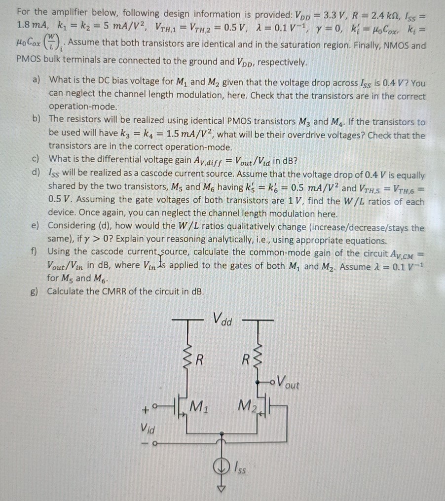
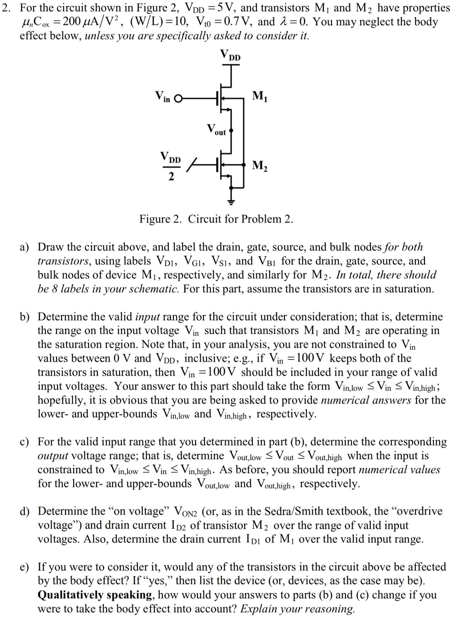
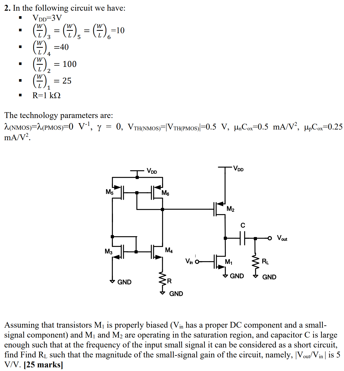
For the amplifier below, following design information is provided: VDD = 3.3 V, R = 2.4 kΩ, ISS = 1.8 mA, k1 = k2 = 5 mA/V2, VTH,1 = VTH,2 = 0.5 V, λ = 0.1 V−1, γ = 0, ki′ = μ0Cox, ki = μ0 Cox(W L)i. Assume that both transistors are identical and in the saturation region. Finally, NMOS and PMOS bulk terminals are connected to the ground and VDD, respectively. a) What is the DC bias voltage for M1 and M2 given that the voltage drop across ISS is 0.4 V ? You can neglect the channel length modulation, here. Check that the transistors are in the correct operation-mode. b) The resistors will be realized using identical PMOS transistors M3 and M4. If the transistors to be used will have k3 = k4 = 1.5 mA/V2, what will be their overdrive voltages? Check that the transistors are in the correct operation-mode. c) What is the differential voltage gain AV,diff = Vout/Vid in dB ? d) ISS will be realized as a cascode current source. Assume that the voltage drop of 0.4 V is equally shared by the two transistors, M5 and M6 having k5′ = k6′ = 0.5 mA/V2 and VTH, 5 = VTH, 6 = 0.5 V. Assuming the gate voltages of both transistors are 1 V, find the W/L ratios of each device. Once again, you can neglect the channel length modulation here. e) Considering (d), how would the W/L ratios qualitatively change (increase/decrease/stays the same), if γ > 0 ? Explain your reasoning analytically, i. e. , using appropriate equations. f) Using the cascode current source, calculate the common-mode gain of the circuit AV, CM = Vout /Vin in dB, where Vin . s applied to the gates of both M1 and M2. Assume λ = 0.1 V−1 for M5 and M6. g) Calculate the CMRR of the circuit in dB.