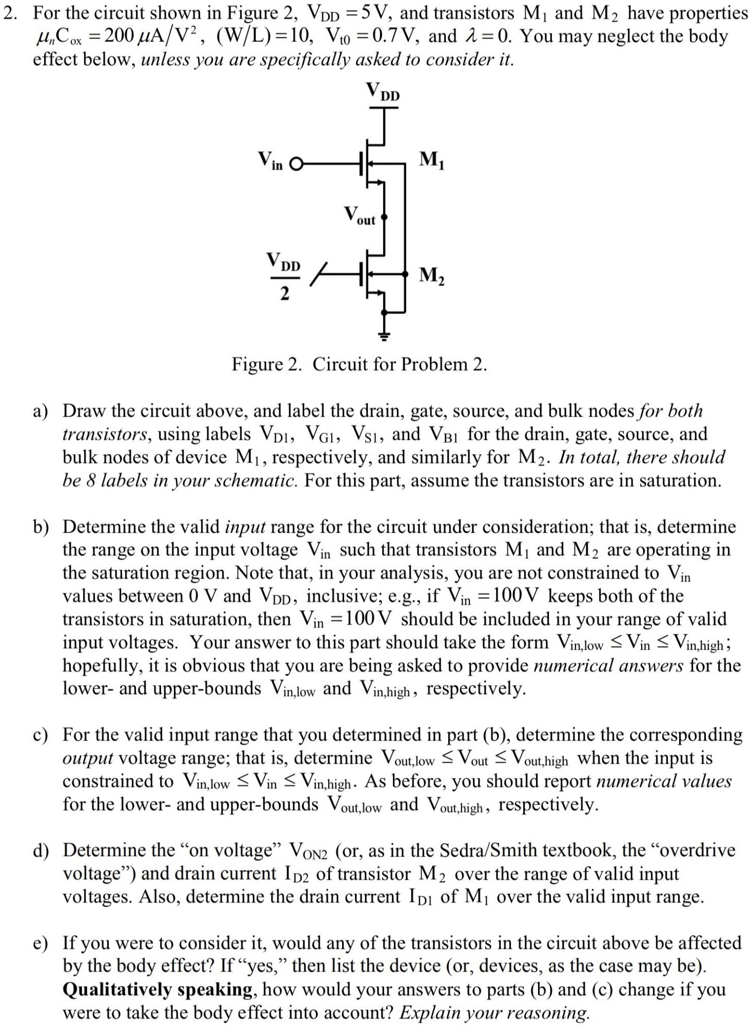
For the circuit shown in Figure 2, VDD = 5 V, and transistors M1 and M2 have properties µnCox = 200µA/V2, (W/L) = 10, Vt0 = 0.7 V, and λ = 0. You may neglect the body effect below, unless you are specifically asked to consider it. Figure 2. Circuit for Problem 2. a) Draw the circuit above, and label the drain, gate, source, and bulk nodes for both transistors, using labels VD1, VG1, VS1, and VB1 for the drain, gate, source, and bulk nodes of device M1, respectively, and similarly for M2. In total, there should be 8 labels in your schematic. For this part, assume the transistors are in saturation. b) Determine the valid input range for the circuit under consideration; that is, determine the range on the input voltage Vin such that transistors M1 and M2 are operating in the saturation region. Note that, in your analysis, you are not constrained to Vin values between 0 V and VDD, inclusive; e.g., if Vin = 100 V keeps both of the transistors in saturation, then Vin = 100 V should be included in your range of valid input voltages. Your answer to this part should take the form Vin,low ≤ Vin ≤ Vin,high ; hopefully, it is obvious that you are being asked to provide numerical answers for the lower- and upper-bounds Vin,low and Vin,high , respectively. c) For the valid input range that you determined in part (b), determine the corresponding output voltage range; that is, determine Vout,low ≤ Vout ≤ Vout,high when the input is constrained to Vin,low ≤ Vin ≤ Vin,high. . As before, you should report numerical values for the lower- and upper-bounds Vout,low and Vout,high, , respectively. d) Determine the "on voltage" VON2 (or, as in the Sedra/Smith textbook, the "overdrive voltage") and drain current ID2 of transistor M2 over the range of valid input voltages. Also, determine the drain current ID1 of M1 over the valid input range. e) If you were to consider it, would any of the transistors in the circuit above be affected by the body effect? If "yes," then list the device (or, devices, as the case may be). Qualitatively speaking, how would your answers to parts (b) and (c) change if you were to take the body effect into account? Explain your reasoning.
Image text
For the circuit shown in Figure 2, VDD = 5 V, and transistors M1 and M2 have properties µnCox = 200µA/V2, (W/L) = 10, Vt0 = 0.7 V, and λ = 0. You may neglect the body effect below, unless you are specifically asked to consider it. Figure 2. Circuit for Problem 2. a) Draw the circuit above, and label the drain, gate, source, and bulk nodes for both transistors, using labels VD1, VG1, VS1, and VB1 for the drain, gate, source, and bulk nodes of device M1, respectively, and similarly for M2. In total, there should be 8 labels in your schematic. For this part, assume the transistors are in saturation. b) Determine the valid input range for the circuit under consideration; that is, determine the range on the input voltage Vin such that transistors M1 and M2 are operating in the saturation region. Note that, in your analysis, you are not constrained to Vin values between 0 V and VDD, inclusive; e.g., if Vin = 100 V keeps both of the transistors in saturation, then Vin = 100 V should be included in your range of valid input voltages. Your answer to this part should take the form Vin,low ≤ Vin ≤ Vin,high ; hopefully, it is obvious that you are being asked to provide numerical answers for the lower- and upper-bounds Vin,low and Vin,high , respectively. c) For the valid input range that you determined in part (b), determine the corresponding output voltage range; that is, determine Vout,low ≤ Vout ≤ Vout,high when the input is constrained to Vin,low ≤ Vin ≤ Vin,high. . As before, you should report numerical values for the lower- and upper-bounds Vout,low and Vout,high, , respectively. d) Determine the "on voltage" VON2 (or, as in the Sedra/Smith textbook, the "overdrive voltage") and drain current ID2 of transistor M2 over the range of valid input voltages. Also, determine the drain current ID1 of M1 over the valid input range. e) If you were to consider it, would any of the transistors in the circuit above be affected by the body effect? If "yes," then list the device (or, devices, as the case may be). Qualitatively speaking, how would your answers to parts (b) and (c) change if you were to take the body effect into account? Explain your reasoning.


![For the circuit shown in Figure 1, NMOS device M1 has the following properties: kn’(W/L) = 180 μA/V2, VT0 = 2 V, λ = 0.02 V-1, γ = 0.4 V1/2, 2ϕF = 0.7 V, and ID = 10 mA. Note that capacitor Cbig is a DC blocking cap, i.e., Cbig is an open at DC and a short at all other frequencies. Figure 1. Circuit for Problem 1. a) Determine the numerical value of bias voltage Vbias which is needed to achieve a drain current of ID = 10 mA. b) Draw the small-signal equivalent circuit. c) Analyze the small-signal circuit to find Rin, Rout, and Av = Vout/Vin. Find the analytic expression for each quantity first, before determining the numerical answers. d) Recall that gmb/gm = χ. Determine the numerical value of χ for this problem. [Note that this part has nothing to do with parts (b) and (c).] e) What is the threshold voltage of device M1? [Note that this part has nothing to do with parts (b) and (c).] Show your work, list all numerical values in proper engineering notation format with appropriate units and with at least two decimal places of precision.](https://www.doubtrix.com/js/ckeditor/filemanager/connectors/php/editor/1701531864-Rjgbdog0ehds.png)