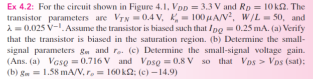
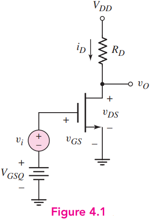
For the circuit shown in Figure 4.1, the transistor parameters are VT N = 0.6 V, kn’ = 80 μA/V2, and λ = 0.015 V-1. Let VDD = 5 V. (a) Design the transistor width-to-length ratio W/L and the resistance RD such that IDQ = 0.5 mA, VGSQ = 1.2 V, and VDSQ = 3 V. (b) Determine gm and ro. (c) Determine the small-signal voltage gain Av = vo/vi.


You'll get a detailed, step-by-step and expert verified solution.
 Work With Experts to Reach at Correct Answers