For the CMOS inverter with given voltage transfer characteristics and schematic, a) Find (VI, VO) in terms of VDD, VTn, VTp, Kn, Kp, and VM at points A, B, C, and D. For points B and C, use VM as the value of VI. b) Determine the states of the transistors in each region (I-to-V). Note that region III corresponds to the line between points B and C. You do not need to verify the states c) Derive VM in terms of VDD, VTn, VTp, Kn, and Kp. For VDD = 5 V and VTn = |VTP| = 1 V, find Kn/Kp to design a CMOS inverter with VM = 0.6 VDD = 3 V.
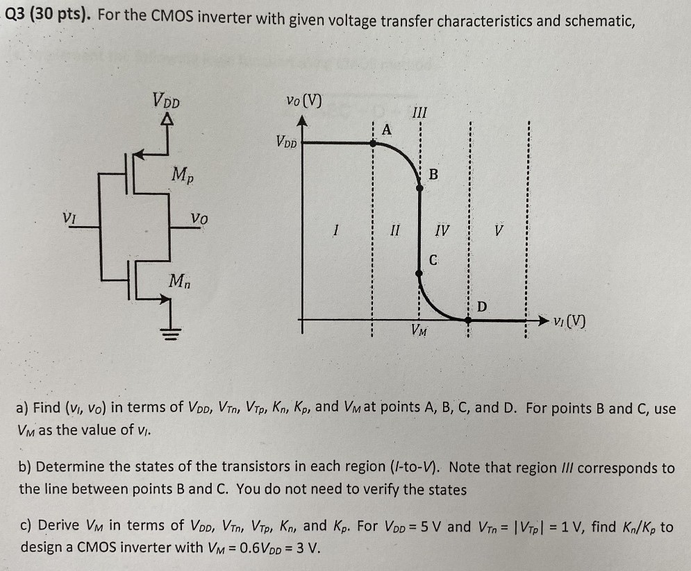
For the CMOS inverter with given voltage transfer characteristics and schematic, a) Find (VI, VO) in terms of VDD, VTn, VTp, Kn, Kp, and VM at points A, B, C, and D. For points B and C, use VM as the value of VI. b) Determine the states of the transistors in each region (I-to-V). Note that region III corresponds to the line between points B and C. You do not need to verify the states c) Derive VM in terms of VDD, VTn, VTp, Kn, and Kp. For VDD = 5 V and VTn = |VTP| = 1 V, find Kn/Kp to design a CMOS inverter with VM = 0.6 VDD = 3 V.

Image text
Q3 (30 pts). For the CMOS inverter with given voltage transfer characteristics and schematic, a) Find ( v 1 , v 0 ) in terms of V D D , V T n , V T p , K n , K p , and V M at points A , B , C , and D . For points B and C , use V M as the value of v 1 . b) Determine the states of the transistors in each region (I-to- V ). Note that region III corresponds to the line between points B and C . You do not need to verify the states c) Derive V M in terms of V D D , V T n , V T p , K n , and K p . For V D D = 5 V and V T n = | V T P | = 1 V , find K n / K p to design a CMOS inverter with V M = 0.6 V D D = 3 V .

Detailed Answer