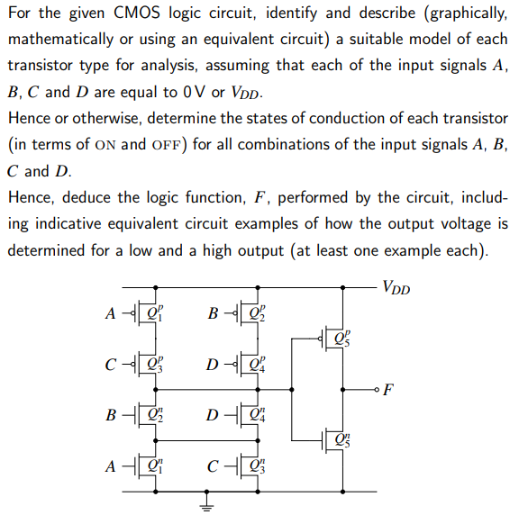
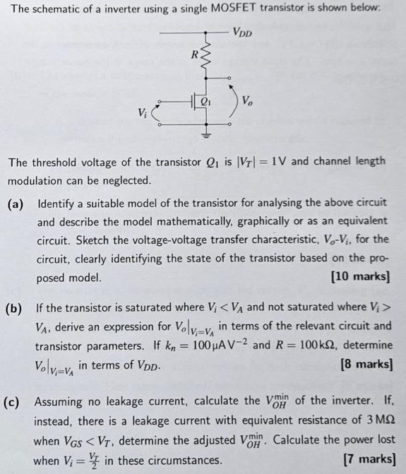
For the given CMOS logic circuit, identify and describe (graphically, mathematically or using an equivalent circuit) a suitable model of each transistor type for analysis, assuming that each of the input signals A, B, C and D are equal to 0 V or VDD. Hence or otherwise, determine the states of conduction of each transistor (in terms of ON and OFF) for all combinations of the input signals A, B, C and D. Hence, deduce the logic function, F, performed by the circuit, including indicative equivalent circuit examples of how the output voltage is determined for a low and a high output (at least one example each).
Image text
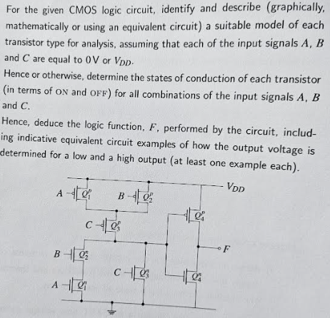
For the given CMOS logic circuit, identify and describe (graphically, mathematically or using an equivalent circuit) a suitable model of each transistor type for analysis, assuming that each of the input signals A, B, C and D are equal to 0 V or VDD. Hence or otherwise, determine the states of conduction of each transistor (in terms of ON and OFF) for all combinations of the input signals A, B, C and D. Hence, deduce the logic function, F, performed by the circuit, including indicative equivalent circuit examples of how the output voltage is determined for a low and a high output (at least one example each).