For the JFET biasing shown in Figur:8-16(a), determine the values of ID, VGS and VDS given that IDSS = 3 mA, VGS (off) = −2.4 V, RG = 10 MΩ and VDD = 10 V, RS = 350 Ω, RD = 1.9 KΩ. (a) n channel (b) p channel FIGURE 8−16 Self-biased JFETs (IS = ID in all FETs ).
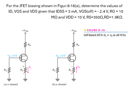
For the JFET biasing shown in Figur:8-16(a), determine the values of ID, VGS and VDS given that IDSS = 3 mA, VGS (off) = −2.4 V, RG = 10 MΩ and VDD = 10 V, RS = 350 Ω, RD = 1.9 KΩ. (a) n channel (b) p channel FIGURE 8−16 Self-biased JFETs (IS = ID in all FETs ).

Image text
For the JFET biasing shown in Figur:8-16(a), determine the values of ID, VGS and VDS given that IDSS = 3 m A , V G S (off) = 2.4 V , R G = 10 M Ω and V D D = 10 V , R S = 350 Ω , R D = 1.9 K Ω . (a) n chansel (b) p channel 4 FIGURE 8 16 Self-biased JFETs ( I S = I D in all FETs ) .

Detailed Answer