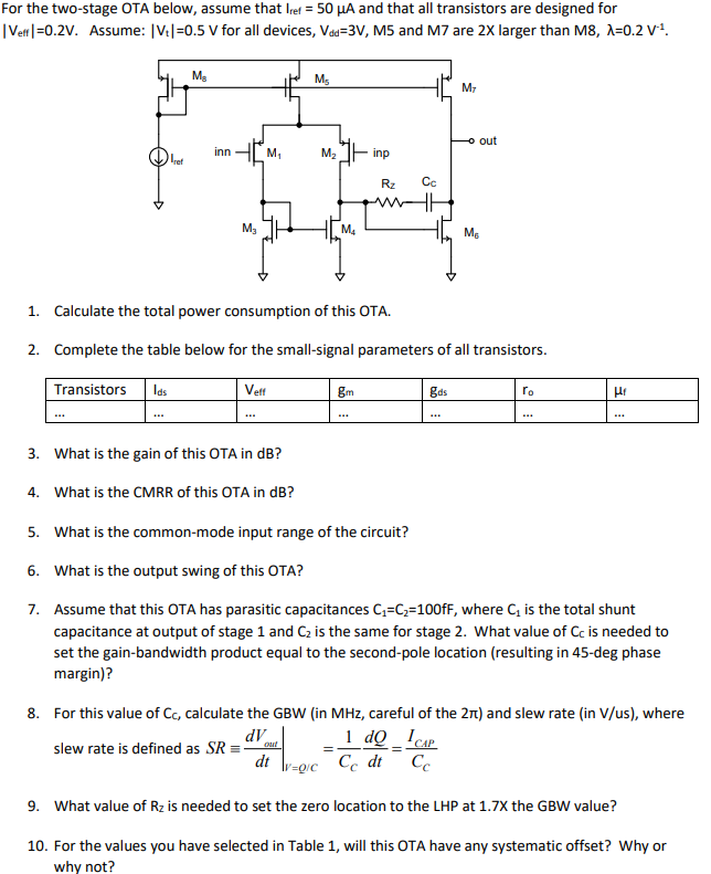
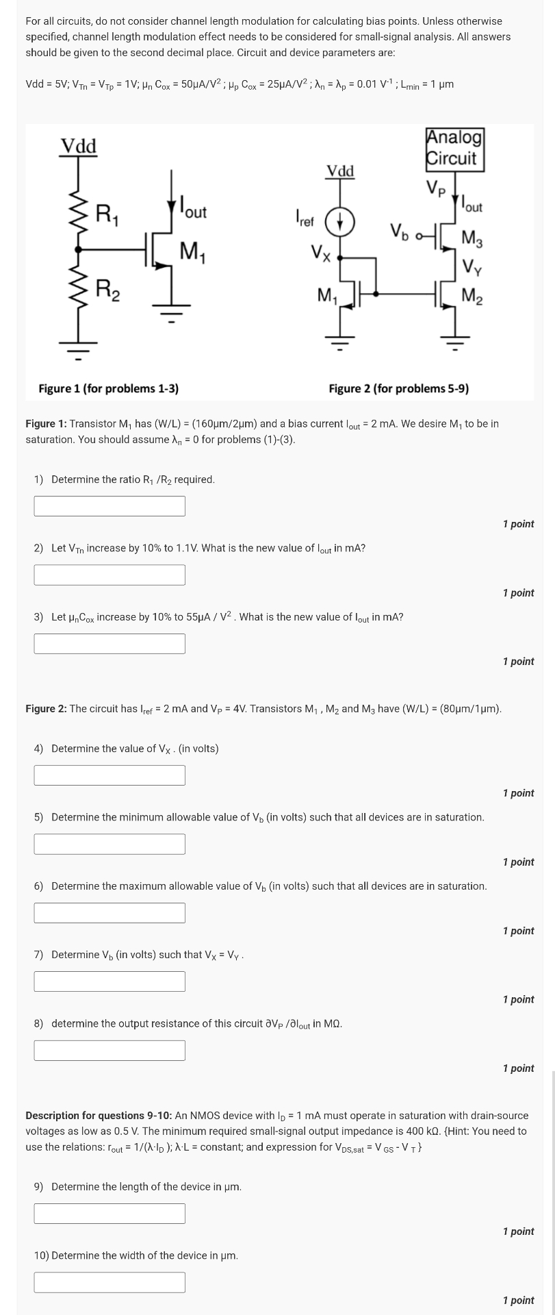
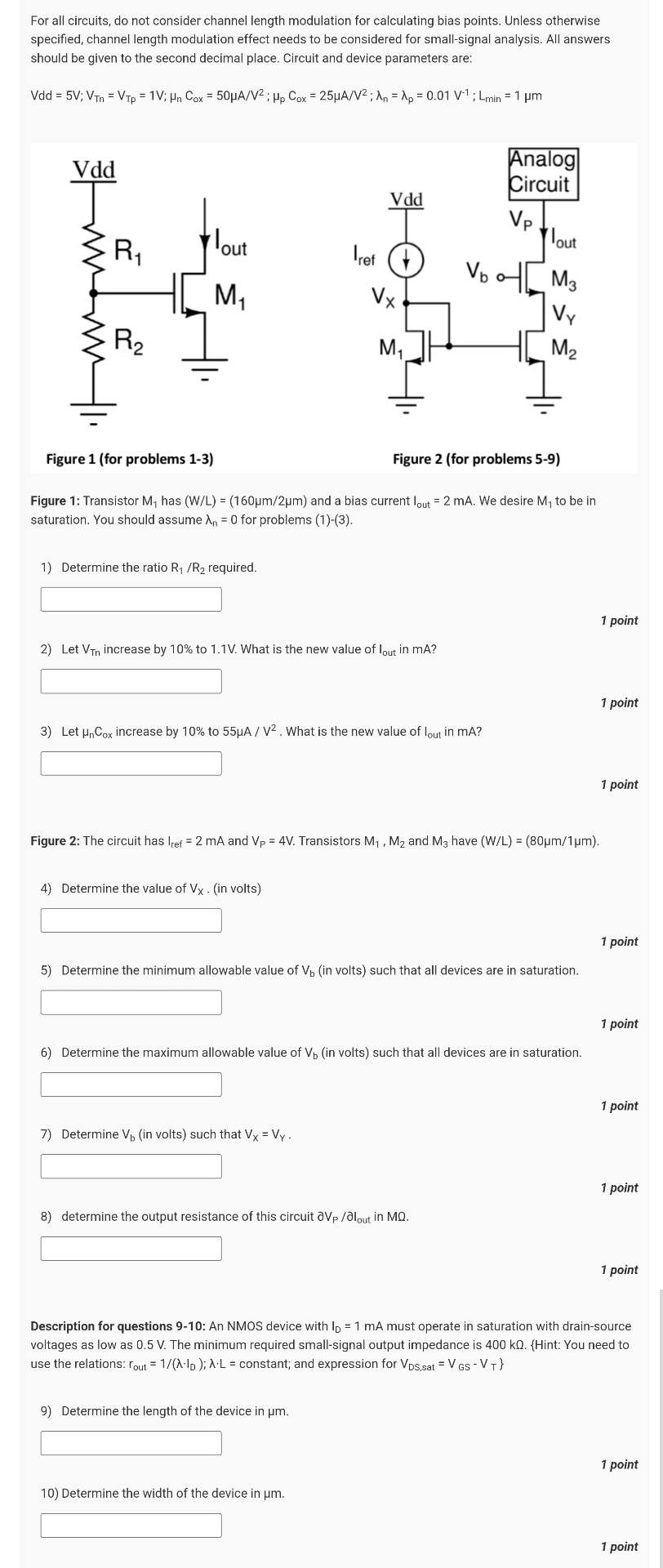
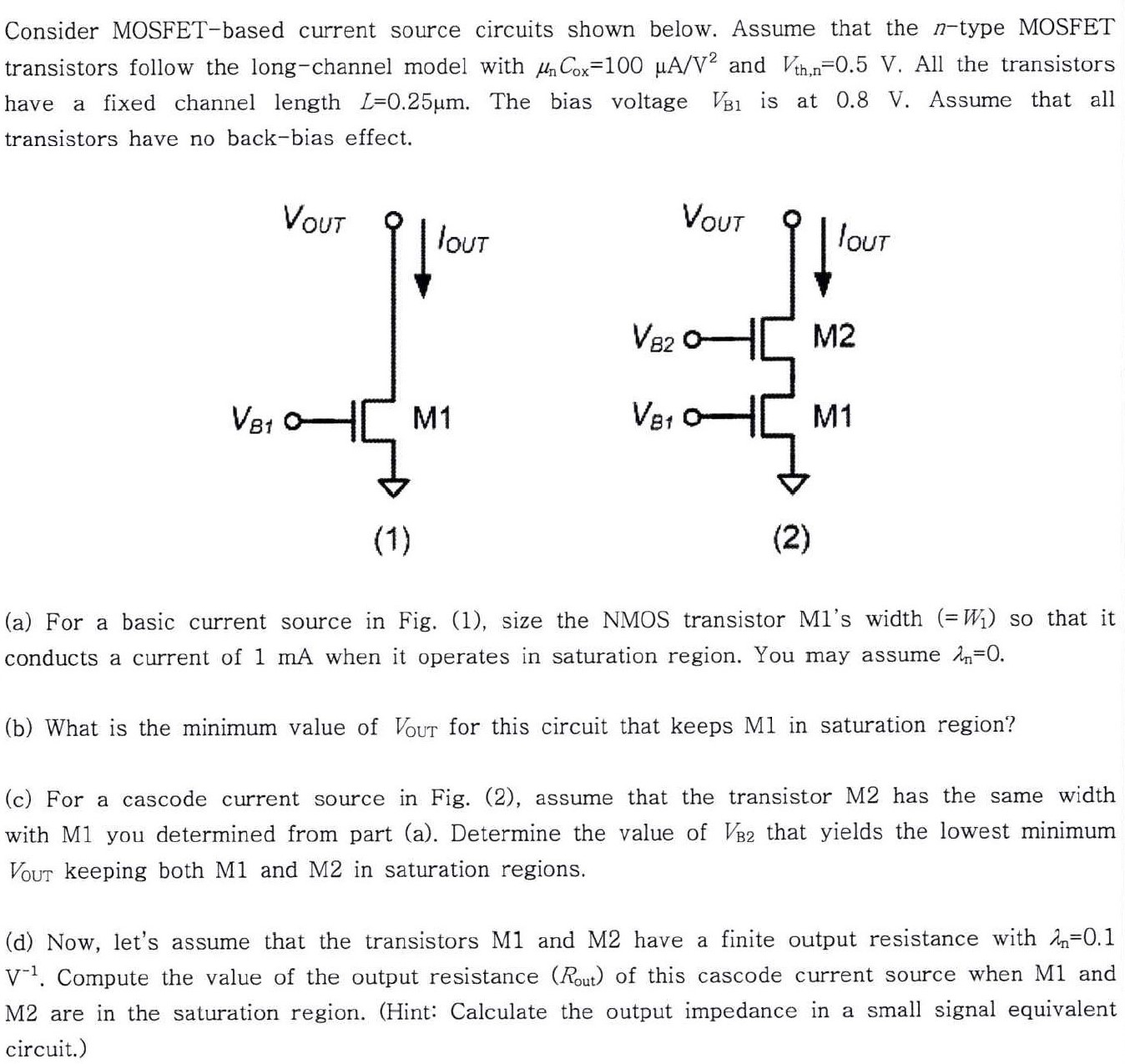
For the two-stage OTA below, assume that Iref = 50 μA and that all transistors are designed for |Veff|= 0.2 V. Assume: |Vt|= 0.5 V for all devices, Vdd = 3 V, M5 and M7 are 2X larger than M8, λ = 0.2V-1. 1. Calculate the total power consumption of this OTA. 2. Complete the table below for the small-signal parameters of all transistors. Transistors Ids Veff gm gds ro μf 3. What is the gain of this OTA in dB? 4. What is the CMRR of this OTA in dB? 5. What is the common-mode input range of the circuit? 6. What is the output swing of this OTA? 7. Assume that this OTA has parasitic capacitances C1 = C2 = 100fF, where C1 is the total shunt capacitance at output of stage 1 and C2 is the same for stage 2. What value of Cc is needed to set the gain-bandwidth product equal to the second-pole location (resulting in 45-deg phase margin)? 8. For this value of Cc, calculate the GBW (in MHz, careful of the 2π ) and slew rate (in V/us), where slew rate is defined as 9. What value of RZ is needed to set the zero location to the LHP at 1.7X the GBW value? 10. For the values you have selected in Table 1, will this OTA have any systematic offset? Why or why not?
Image text
For the two-stage OTA below, assume that Iref = 50 μA and that all transistors are designed for |Veff|= 0.2 V. Assume: |Vt|= 0.5 V for all devices, Vdd = 3 V, M5 and M7 are 2X larger than M8, λ = 0.2V-1. 1. Calculate the total power consumption of this OTA. 2. Complete the table below for the small-signal parameters of all transistors. Transistors Ids Veff gm gds ro μf 3. What is the gain of this OTA in dB? 4. What is the CMRR of this OTA in dB? 5. What is the common-mode input range of the circuit? 6. What is the output swing of this OTA? 7. Assume that this OTA has parasitic capacitances C1 = C2 = 100fF, where C1 is the total shunt capacitance at output of stage 1 and C2 is the same for stage 2. What value of Cc is needed to set the gain-bandwidth product equal to the second-pole location (resulting in 45-deg phase margin)? 8. For this value of Cc, calculate the GBW (in MHz, careful of the 2π ) and slew rate (in V/us), where slew rate is defined as 9. What value of RZ is needed to set the zero location to the LHP at 1.7X the GBW value? 10. For the values you have selected in Table 1, will this OTA have any systematic offset? Why or why not?