Give the truth table for the following transistor level schematic. Explain the source of "good logic 0’s i.e., GND" and "good logic 1 ’s i.e., VDD" (using the labels P1, P2, N1 and N2) at C under each of the four input conditions ( AB = 00, 01, 10, 11). A B OUT Source of Good Logic 0 at C Source of Good Logic 1 at C 0 0 0 1 1 1 1 0
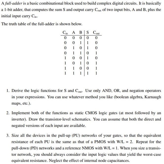
Image text
Give the truth table for the following transistor level schematic. Explain the source of "good logic 0’s i.e., GND" and "good logic 1 ’s i.e., VDD" (using the labels P1, P2, N1 and N2) at C under each of the four input conditions ( AB = 00, 01, 10, 11). A B OUT Source of Good Logic 0 at C Source of Good Logic 1 at C 0 0 0 1 1 1 1 0


![Question 8. [10 marks] Design a CMOS amplifier using the configuration shown to give an input resistance of 1 MΩ and a voltage gain of at least vOUT/vIN = −5 V/V to a load resistance of 10 kΩ. Let VDD = 5 V, k′W/L = 0.5 mA/V2, |Vt| = 1, and VA = 50 V for all transistors, and assume that C → ∞. Give −VSS and R to provide the required gain. R : 5 kΩ −VSS: VSS = −3 V Figure 4: Common source amplifier.](https://www.doubtrix.com/uploads/editor/5768063169qDHrlsUpFB.png)