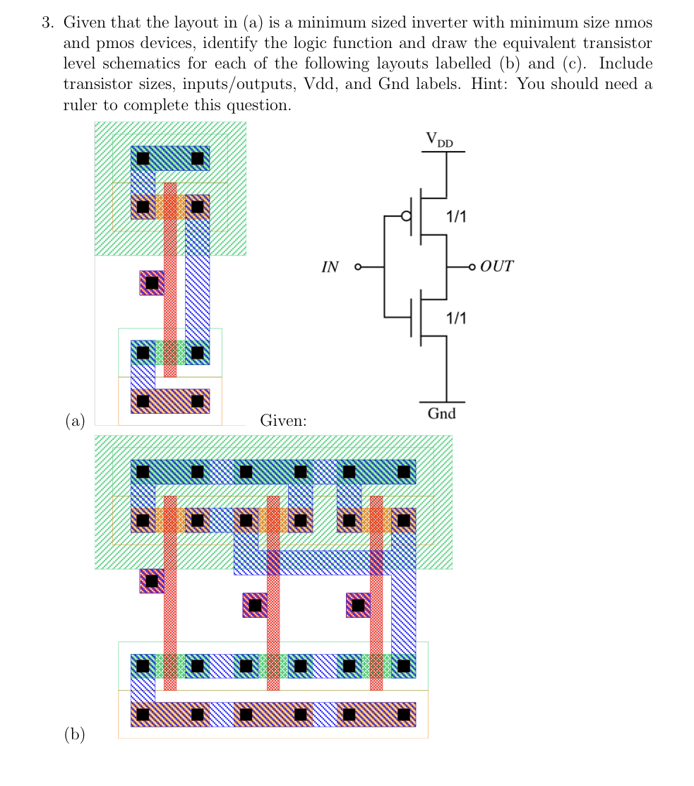
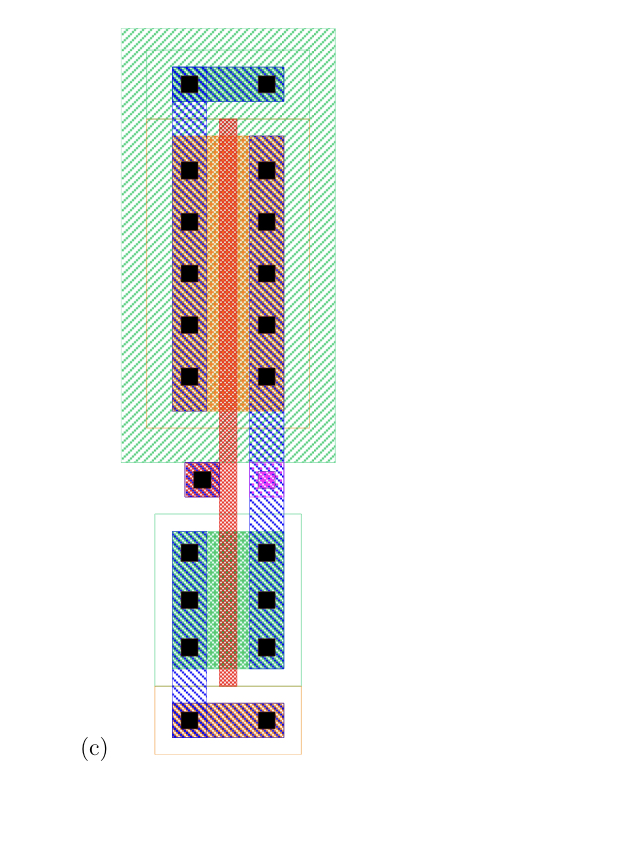
Given that the layout in (a) is a minimum sized inverter with minimum size nmos and pmos devices, identify the logic function and draw the equivalent transistor level schematics for each of the following layouts labelled (b) and (c). Include transistor sizes, inputs/outputs, Vdd, and Gnd labels. Hint: You should need a ruler to complete this question.

You'll get a detailed, step-by-step and expert verified solution.
 Work With Experts to Reach at Correct Answers