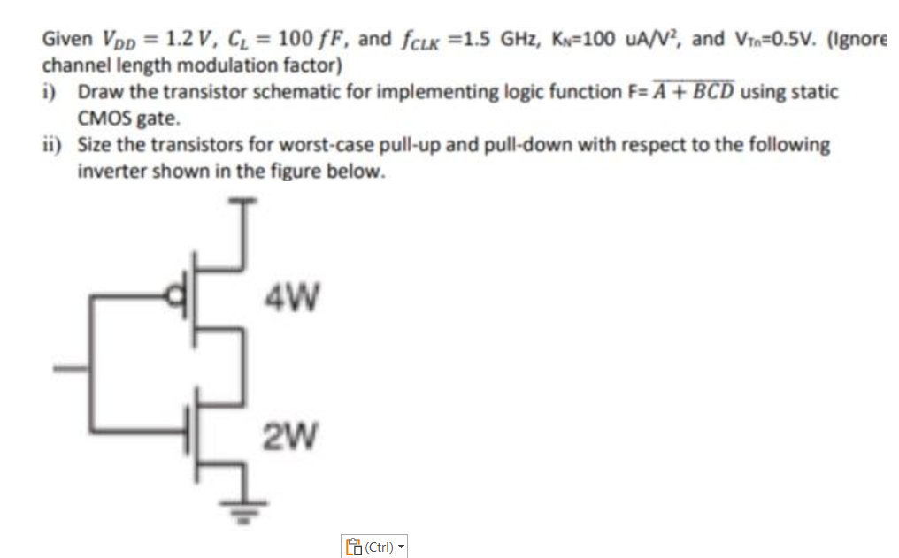
Given VDD = 1.2 V, CL = 100 fF, and fCLK = 1.5 GHz, KN = 100 uA/V2, and VTn = 0.5 V. (Ignore channel length modulation factor) i) Draw the transistor schematic for implementing logic function F = A+BCD using static CMOS gate. ii) Size the transistors for worst-case pull-up and pull-down with respect to the following inverter shown in the figure below.