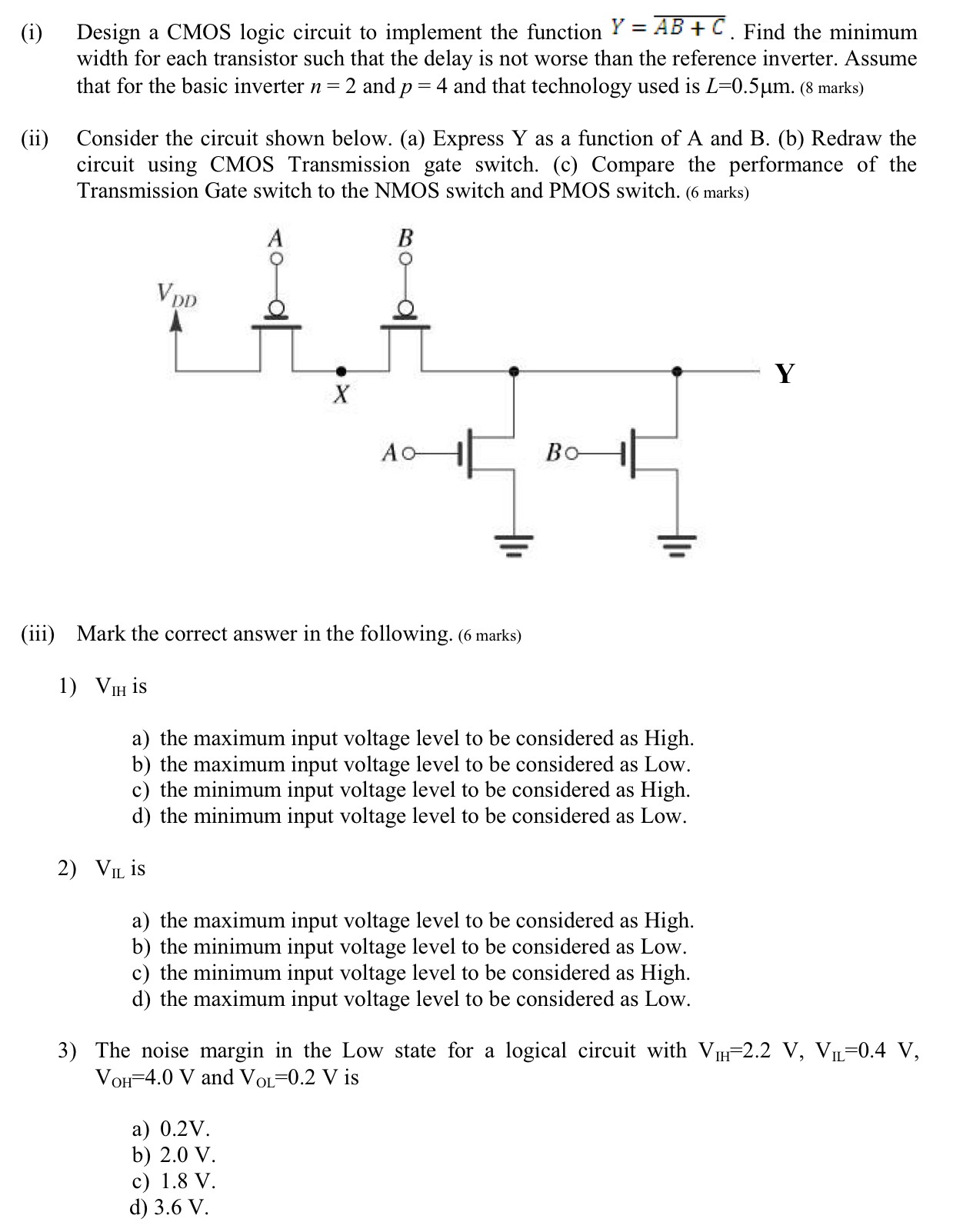
(i) Design a CMOS logic circuit to implement the function Y = AB + C¯. Find the minimum width for each transistor such that the delay is not worse than the reference inverter. Assume that for the basic inverter n = 2 and p = 4 and that technology used is L = 0.5 μm. ( 8 marks) (ii) Consider the circuit shown below. (a) Express Y as a function of A and B. (b) Redraw the circuit using CMOS Transmission gate switch. (c) Compare the performance of the Transmission Gate switch to the NMOS switch and PMOS switch. (6 marks) (iii) Mark the correct answer in the following. (6 marks)VIH is a) the maximum input voltage level to be considered as High. b) the maximum input voltage level to be considered as Low. c) the minimum input voltage level to be considered as High. d) the minimum input voltage level to be considered as Low. VIL is a) the maximum input voltage level to be considered as High. b) the minimum input voltage level to be considered as Low. c) the minimum input voltage level to be considered as High. d) the maximum input voltage level to be considered as Low. The noise margin in the Low state for a logical circuit with VIH = 2.2 V, VIL = 0.4 V, VOH = 4.0 V and VOL = 0.2 V is a) 0.2 V. b) 2.0 V c) 1.8 V. d) 3.6 V.