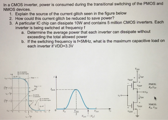
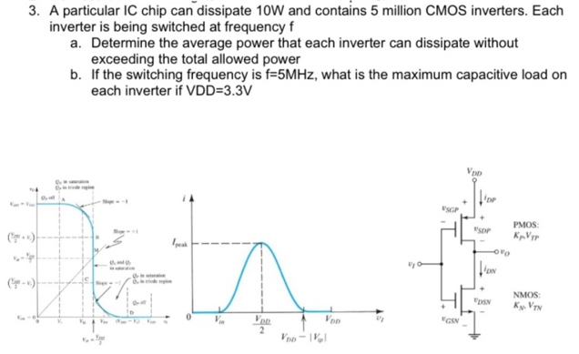
In a CMOS inverter, power is consumed during the transitional switching of the PMOS and NMOS devices. Explain the source of the current glitch seen in the figure belowHow could this current glitch be reduced to save power? A particular IC chip can dissipate 10 W and contains 5 million CMOS inverters. Each inverter is being switched at frequency f a. Determine the average power that each inverter can dissipate without exceeding the total allowed power b. If the switching frequency is f = 5 MHz, what is the maximum capacitive load on each inverter if VDD = 3.3 V