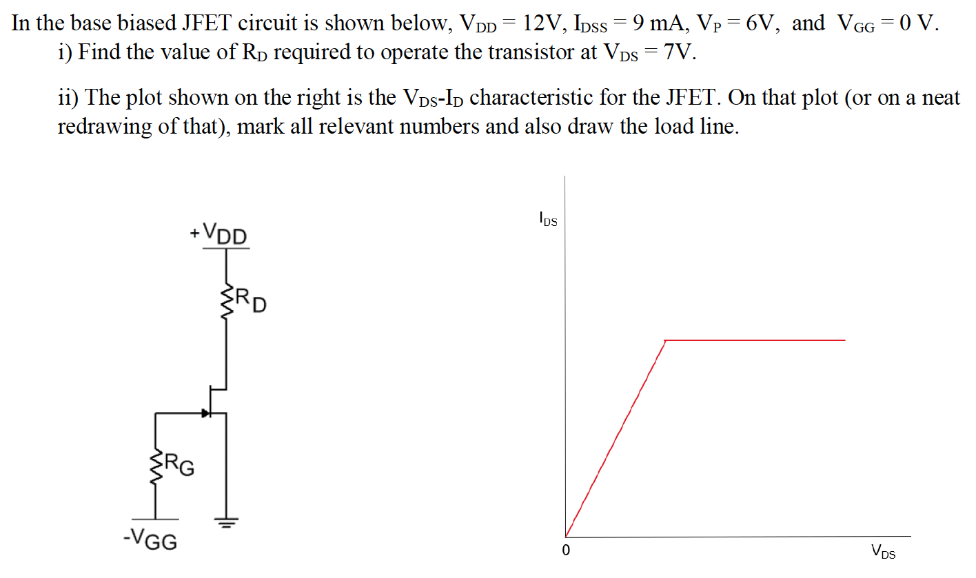
In the base biased JFET circuit is shown below, VDD = 12 V, IDSS = 9 mA, VP = 6 V, and VGG = 0 V. i) Find the value of RD required to operate the transistor at VDS = 7 V. ii) The plot shown on the right is the VDS−ID characteristic for the JFET. On that plot (or on a neat redrawing of that), mark all relevant numbers and also draw the load line.
