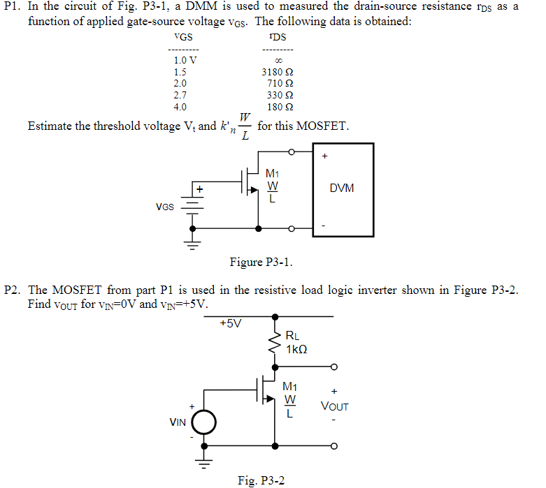
In the circuit of Fig. P3-1, a DMM is used to measured the drain-source resistance rDS as a function of applied gate-source voltage VGS. The following data is obtained: Estimate the threshold voltage Vt and kn’W/L for this MOSFET. Figure P3-1. P2. The MOSFET from part P1 is used in the resistive load logic inverter shown in Figure P3-2. Find vOUT for vIN = 0 V and vIN = +5 V. Fig. P3-2 vGS rDS 1.0 V ∞ 1.5 3180Ω 2.0 710Ω 2.7 330Ω 4.0 180Ω


You'll get a detailed, step-by-step and expert verified solution.
 Work With Experts to Reach at Correct Answers