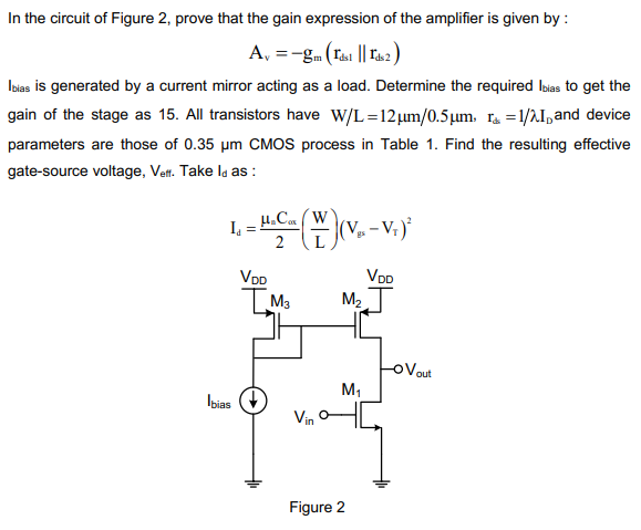
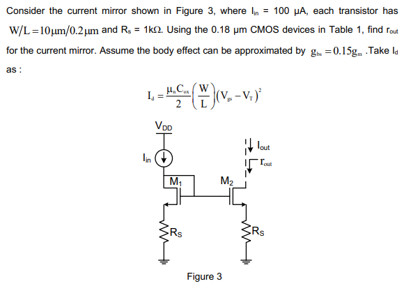
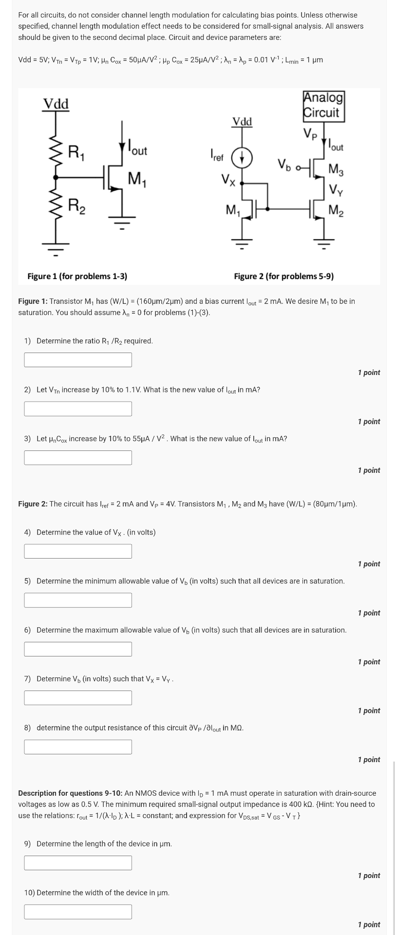
In the circuit of Figure 2, prove that the gain expression of the amplifier is given by : Av = −gm(rds1∥rds) I bias is generated by a current mirror acting as a load. Determine the required Ibias to get the gain of the stage as 15. All transistors have W/L = 12 μm/0.5 μm, rΔ = 1 /λID and device parameters are those of 0.35 μm CMOS process in Table 1. Find the resulting effective gate-source voltage, Veff. Take Id as : Id = μnCox 2 (W L)(Vgs − VT)2 Figure 2