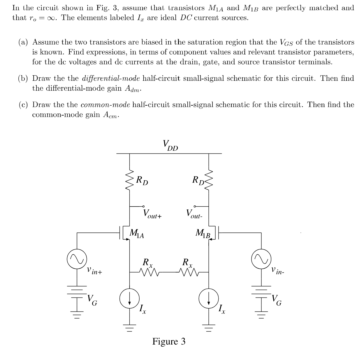
In the circuit shown in Fig. 3, assume that transistors M1 A and M1 B are perfectly matched and that ro = ∞. The elements labeled Ix are ideal DC current sources. (a) Assume the two transistors are biased in the saturation region that the VGS of the transistors is known. Find expressions, in terms of component values and relevant transistor parameters, for the dc voltages and dc currents at the drain, gate, and source transistor terminals. (b) Draw the the differential-mode half-circuit small-signal schematic for this circuit. Then find the differential-mode gain Adm. (c) Draw the the common-mode half-circuit small-signal schematic for this circuit. Then find the common-mode gain Acm. Figure 3

![(a) Figure Q2(a) shows a differential amplifier with a current source at the bottom. It is given that VDD = VSS = 15 V, ISS = 300 μA, Early effect can be ignored (λ = 0), Kn = 400 μA/V2 and VTN = 1 V. You may assume MOSFET in saturation region. (i) For single ended outputs, draw the half-circuits and derive the algebraic equations for the differential mode and common-mode gains as well as CMRR. [6 Marks] (ii) For the above case of single ended output, what should be the value of Rss to get CMRR = 100? [4 Marks] Figure Q2(a) (b) Figure Q2(b) shows a MOSFET based current mirror. Draw the AC small signal model and derive an equation for output resistance Rout as shown in the figure. You can keep your answer in terms of gm, ro etc but denote the subscript 1,2,3 etc to indicate which transistor. In other words, denote transconductance of M2 by writing gm2 and so on. [6 marks] (c) Draw the diagram of a BJT based Class B push-pull power amplifier and derive the maximum possible power efficiency of this circuit. You may ignore crossover distortion and assume |VCE(sat)| = 0 V. [9 marks]](https://www.doubtrix.com/uploads/editor/1710360410ITbaKcVzzE.jpg)