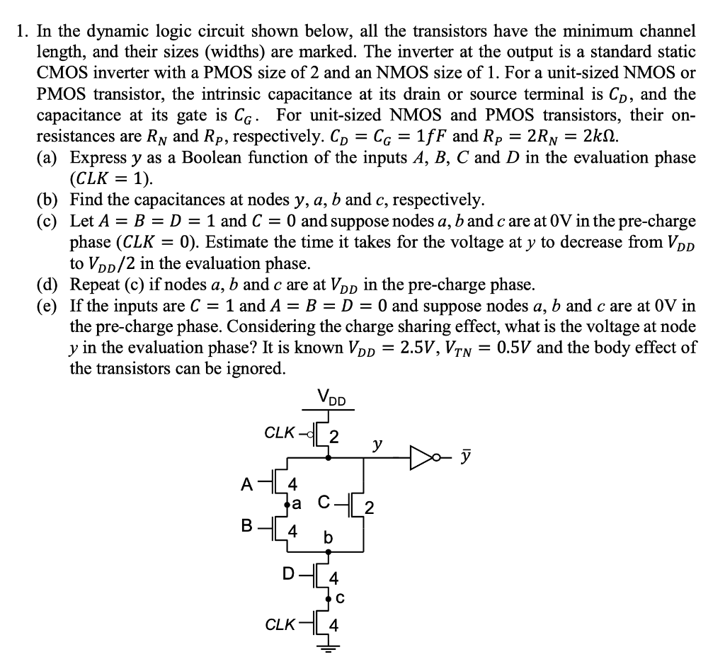
In the dynamic logic circuit shown below, all the transistors have the minimum channel length, and their sizes (widths) are marked. The inverter at the output is a standard static CMOS inverter with a PMOS size of 2 and an NMOS size of 1 . For a unit-sized NMOS or PMOS transistor, the intrinsic capacitance at its drain or source terminal is CD, and the capacitance at its gate is CG. For unit-sized NMOS and PMOS transistors, their onresistances are RN and RP, respectively. CD = CG = 1 fF and RP = 2 RN = 2 kΩ. (a) Express y as a Boolean function of the inputs A, B, C and D in the evaluation phase (CLK = 1). (b) Find the capacitances at nodes y, a, b and c, respectively. (c) Let A = B = D = 1 and C = 0 and suppose nodes a, b and c are at 0 V in the pre-charge phase (CLK = 0). Estimate the time it takes for the voltage at y to decrease from VDD to VDD/2 in the evaluation phase. (d) Repeat (c) if nodes a, b and c are at VDD in the pre-charge phase. (e) If the inputs are C = 1 and A = B = D = 0 and suppose nodes a, b and c are at 0 V in the pre-charge phase. Considering the charge sharing effect, what is the voltage at node y in the evaluation phase? It is known VDD = 2.5 V, VTN = 0.5 V and the body effect of the transistors can be ignored.