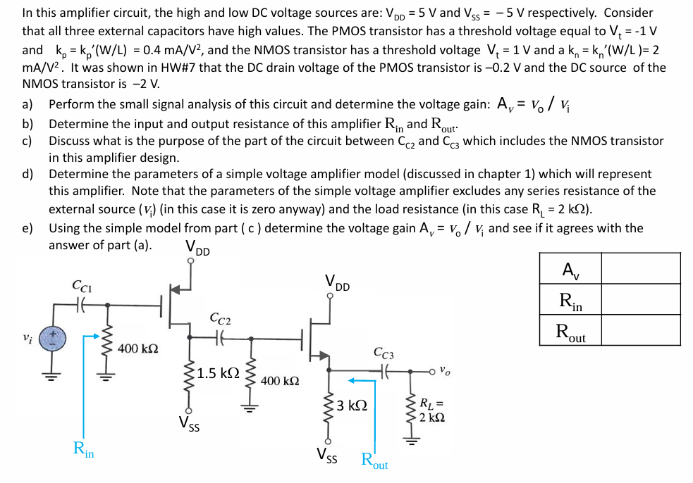
In this amplifier circuit, the high and low DC voltage sources are: VDD = 5 V and VSS = −5 V respectively. Consider that all three external capacitors have high values. The PMOS transistor has a threshold voltage equal to Vt = −1 V and kp = kp′(W/L) = 0.4 mA/V2, and the NMOS transistor has a threshold voltage Vt = 1 V and a kn = kn′(W/L) = 2 mA/V2. It was shown in HW#7 that the DC drain voltage of the PMOS transistor is −0.2 V and the DC source of the NMOS transistor is −2 V. a) Perform the small signal analysis of this circuit and determine the voltage gain: AV = Vo/Vi b) Determine the input and output resistance of this amplifier Rin and Rout . c) Discuss what is the purpose of the part of the circuit between CC2 and CC3 which includes the NMOS transistor in this amplifier design. d) Determine the parameters of a simple voltage amplifier model (discussed in chapter 1) which will represent this amplifier. Note that the parameters of the simple voltage amplifier excludes any series resistance of the external source ( Vi ) (in this case it is zero anyway) and the load resistance (in this case RL = 2 kΩ ). e) Using the simple model from part (c) determine the voltage gain AV = Vo/Vi and see if it agrees with the answer of part (a). VDD

![Q6. For the amplifier circuit shown in Fig. Q6, the MOS Transistor Ml has the following parameters: Kn = 1 mAV−2, and VTHN = 1 V. MOS transistors M2 and M3 are identical and have the following parameters: Kp = 1 mAV−2, and VTHP = −1 V. Fig. Q6 (a) Perform the DC analysis of the amplifier circuit shown in Fig. Q6, and show that the DC gate voltage of Ml is 5 V. You need to explain briefly your answer. (b) Calculate the value of RS such that the drain current of MI is 4 mA. Verify that the Ml is operating in the saturation region. [ Ans: Rs = 0.5 kΩ] (c) Calculate the parameters, gm and ro, of the small-signal model of the transistor Ml. [Ans: gm, M1 = 4 mAV−1, and ro, M1 = ∞ ] (d) What is the configuration of this amplifier? (e) Calculate the values of Rin , and Rout . [Ans: Rin = 5 kΩ and Rout = 2 kΩ ] (f) Estimate the voltage gain, Av( = vout /vin ). [ Ans: AV = −1.78]](https://www.doubtrix.com/uploads/editor/9864219624emwVzDjyOi.png)