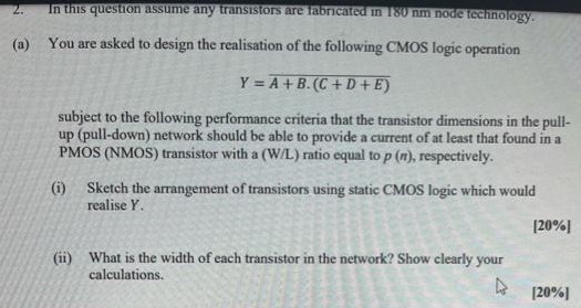
In this question assume any transistors are fabricated in 180 mm node technology. (a) You are asked to design the realisation of the following CMOS logic operation Y = A + B ⋅ (C + D + E) subject to the following performance criteria that the transistor dimensions in the pull-up (pull-down) network should be able to provide a current of at least that found in a PMOS (NMOS) transistor with a (W/L) ratio equal to p(n), respectively. (i) Sketch the arrangement of transistors using static CMOS logic which would realise Y. (ii) What is the width of each transistor in the network? Show clearly your calculations.
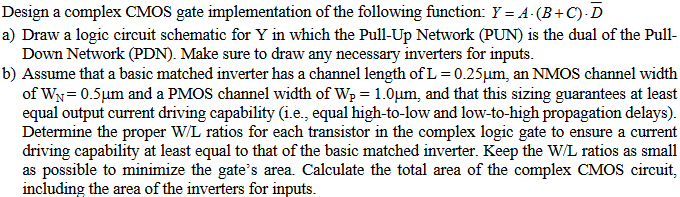
Image text
In this question assume any transistors are fabricated in 180 mm node technology. (a) You are asked to design the realisation of the following CMOS logic operation Y = A + B ⋅ (C + D + E) subject to the following performance criteria that the transistor dimensions in the pull-up (pull-down) network should be able to provide a current of at least that found in a PMOS (NMOS) transistor with a (W/L) ratio equal to p(n), respectively. (i) Sketch the arrangement of transistors using static CMOS logic which would realise Y. (ii) What is the width of each transistor in the network? Show clearly your calculations.