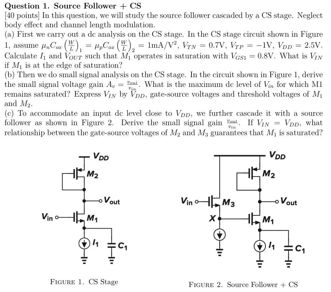
In this question, we will study the source follower cascaded by a CS stage. Neglect body effect and channel length modulation. (a) First we carry out a dc analysis on the CS stage. In the CS stage circuit shown in Figure 1, assume μnCox(W/L)1 = μpCox(W/L)2 = 1mA/V2, VTN = 0.7V, VTP = −1V, VDD = 2.5V. Calculate I1 and VOUT such that M1 operates in saturation with VGS1 = 0.8 V. What is VIN if M1 is at the edge of saturation? (b) Then we do small signal analysis on the CS stage. In the circuit shown in Figure 1, derive the small signal voltage gain Av = vout/vin. What is the maximum dc level of Vin for which M1 remains saturated? Express VIN by VDD, gate-source voltages and threshold voltages of M1 and M2. (c) To accommodate an input de level close to VDD, we further cascade it with a source follower as shown in Figure 2. Derive the small signal gain vout/vin. If VIN = VDD, what relationship between the gate-source voltages of M2 and M3 guarantees that M1 is saturated?

You'll get a detailed, step-by-step and expert verified solution.
 Work With Experts to Reach at Correct Answers