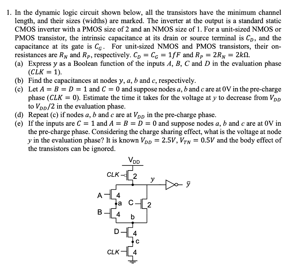
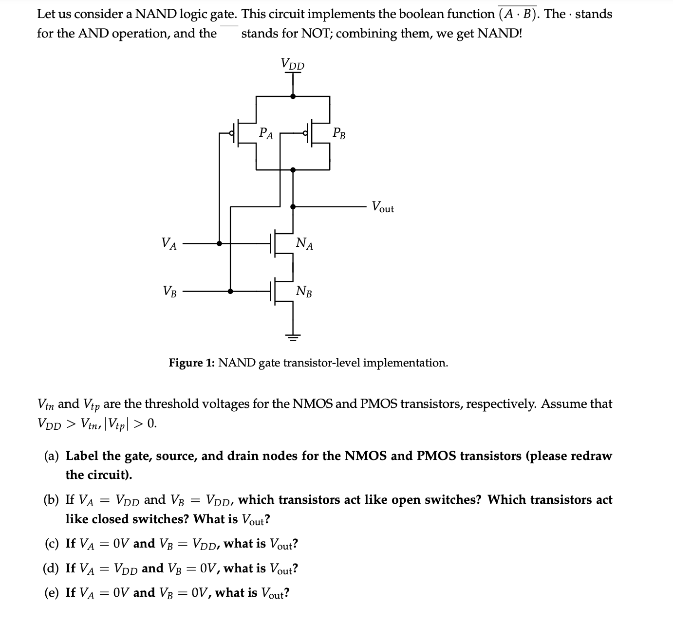
Let us consider a NAND logic gate. This circuit implements the boolean function (A.B). The . stands for the AND operation, and the - stands for NOT; combining them, we get NAND! Figure 1: NAND gate transistor-level implementation. Vtn and Vtp are the threshold voltages for the NMOS and PMOS transistors, respectively. Assume that VDD > Vtn, |Vtp| > 0. (a) Label the gate, source, and drain nodes for the NMOS and PMOS transistors (please redraw the circuit). (b) If VA = VDD and VB = VDD, which transistors act like open switches? Which transistors act like closed switches? What is Vout? (c) If VA = 0V and VB = VDD, what is Vout? (d) If VA = VDD and VB = 0V, what is Vout? (e) If VA = 0V and VB = 0V, what is Vout? (f) Write out the truth table for this circuit.

You'll get a detailed, step-by-step and expert verified solution.
 Work With Experts to Reach at Correct Answers
![Below is a circuit consisting of 2 PMOS and 2 NMOS FETs, labeled 1 through 4. The PMOS has a threshold voltage = -0.1 V. The NMOS has a threshold voltage = +0.1 V. VDD = 2 V. Assume that if a transistor is on, it is saturated (i. e. for that transistor VDS = VGS−VT ). If VA = 0 and VB = 0, what is VGS of FET (1)? Is it on? Justify your answer. [5 points] If VA = 0 and VB = 0, what is VGS of FET (4)? Is it on? Justify your answer. [5 points]](https://www.doubtrix.com/uploads/editor/5103180418zjDezXTaiG.png)