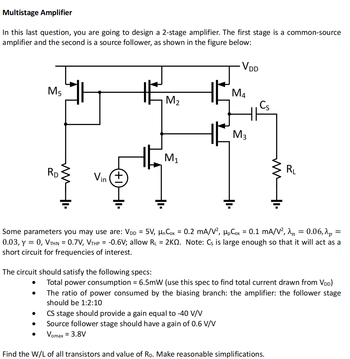
Multistage Amplifier In this last question, you are going to design a 2-stage amplifier. The first stage is a common-source amplifier and the second is a source follower, as shown in the figure below: Some parameters you may use are: VDD = 5 V, μnCox = 0.2 mA/V2, μpCox = 0.1 mA/V2, λn = 0.06, λp = 0.03, γ = 0, VTHN = 0.7 V, VTHP = −0.6 V; allow RL = 2 KΩ. Note: CS is large enough so that it will act as a short circuit for frequencies of interest. The circuit should satisfy the following specs: Total power consumption = 6.5 mW (use this spec to find total current drawn from VDD) The ratio of power consumed by the biasing branch: the amplifier: the follower stage should be 1:2:10 CS stage should provide a gain equal to −40 V/V Source follower stage should have a gain of 0.6 V/V Vomax = 3.8 V Find the W/L of all transistors and value of RD. Make reasonable simplifications.