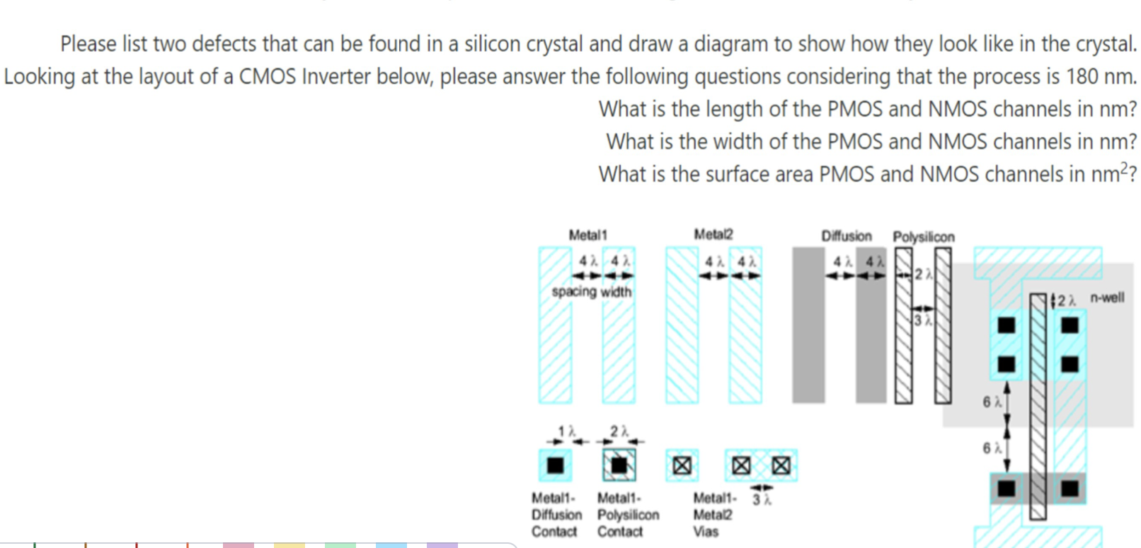
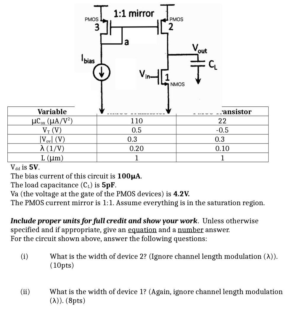
Please list two defects that can be found in a silicon crystal and draw a diagram to show how they look like in the crystal. Looking at the layout of a CMOS Inverter below, please answer the following questions considering that the process is 180 nm. What is the length of the PMOS and NMOS channels in nm? What is the width of the PMOS and NMOS channels in nm? What is the surface area PMOS and NMOS channels in nm^2?
Image text
Please list two defects that can be found in a silicon crystal and draw a diagram to show how they look like in the crystal. Looking at the layout of a CMOS Inverter below, please answer the following questions considering that the process is 180 nm. What is the length of the PMOS and NMOS channels in nm? What is the width of the PMOS and NMOS channels in nm? What is the surface area PMOS and NMOS channels in nm^2?