Please use the 180 nm process parameters shown at the end of homework for all the homework questions. For NMOS as Rn = 6.47 KΩ, for PMOS as Rp = 29.6 KΩ, and C1 = 0.89 fF)Design the static complementary gates (CMOS gates) for the following logic expressions using pull-up/pull-down networks. Use a truth table to show logical equivalence for converted expressions. Assume inverted variables are available, i. e., you do not have to add inverters for complementary variables. (10 pt) a) a+b b) ab c) (a+b)c d) (ab)′+(cd)
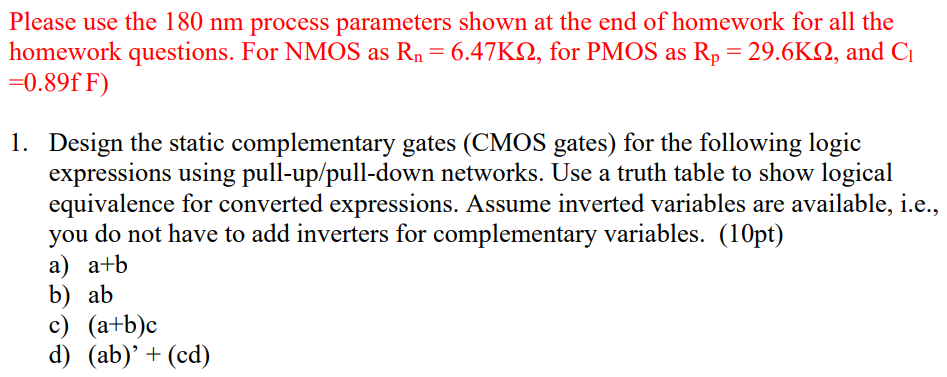
Please use the 180 nm process parameters shown at the end of homework for all the homework questions. For NMOS as Rn = 6.47 KΩ, for PMOS as Rp = 29.6 KΩ, and C1 = 0.89 fF)Design the static complementary gates (CMOS gates) for the following logic expressions using pull-up/pull-down networks. Use a truth table to show logical equivalence for converted expressions. Assume inverted variables are available, i. e., you do not have to add inverters for complementary variables. (10 pt) a) a+b b) ab c) (a+b)c d) (ab)′+(cd)

Image text
Please use the 180 nm process parameters shown at the end of homework for all the homework questions. For NMOS as R n = 6.47 K Ω , for PMOS as R p = 29.6 K Ω , and C 1 = 0.89 fF )
  1. Design the static complementary gates (CMOS gates) for the following logic expressions using pull-up/pull-down networks. Use a truth table to show logical equivalence for converted expressions. Assume inverted variables are available, i.e., you do not have to add inverters for complementary variables. (10pt) a) a + b b) a b c) ( a + b ) c d) ( a b ) + ( c d )

Detailed Answer