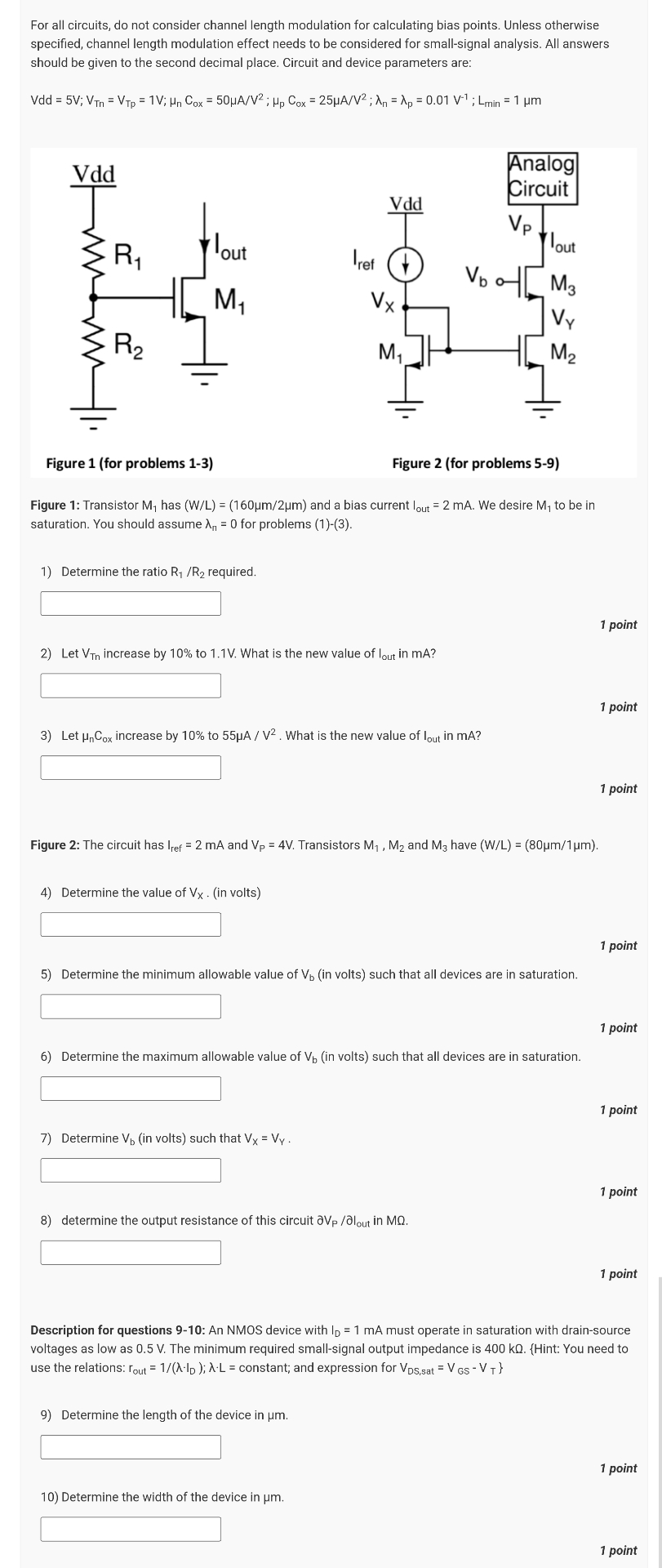
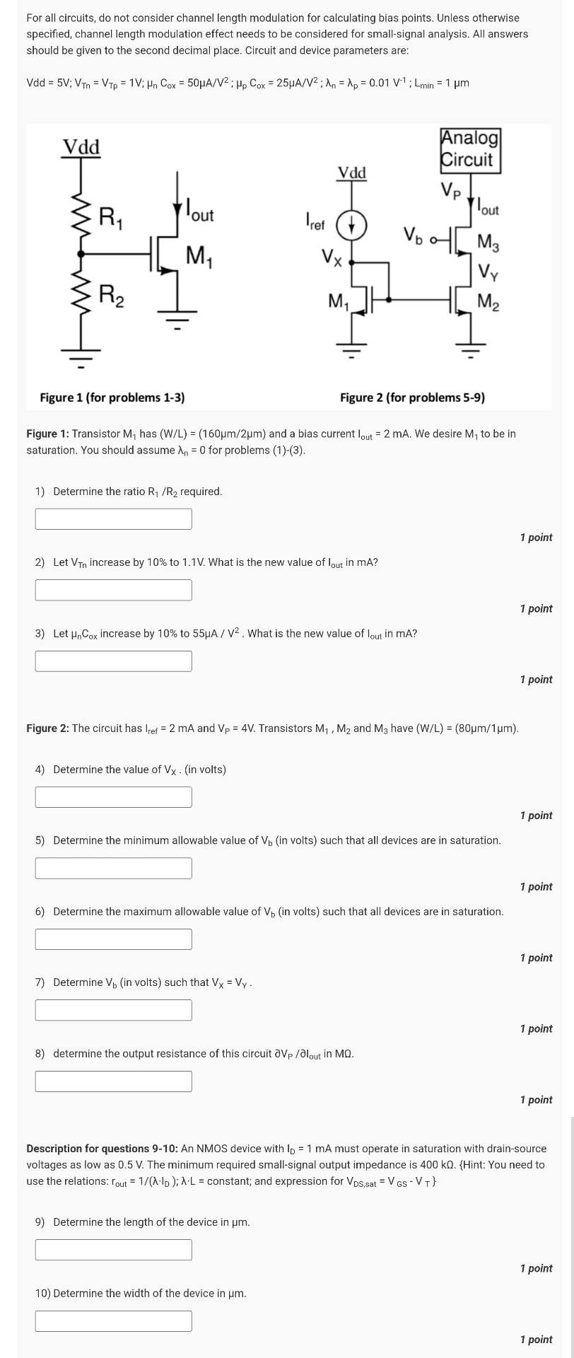
problem 1 Design the inverter (determine the W/L of each device) in Fig. 1 to have a self-bias voltage of 0.9 V and a quiescent current of 108 μA when self-biased. Ignore λ for operating point calculations. What is the dc gain of this inverter? (Use this inverter for the rest of the problems). For the following problems, use the data below: μnCox = 300 μA/V2, μpCox = 75 μA/V2, VTn = VTp = 0.6 V; λp = λn = 0.1 /V Problem 1 Figure 1: Circuit for