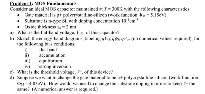
Problem 1: MOS Fundamentals Consider an ideal MOS capacitor maintained at T = 300 K with the following characteristics:Gate material is p+ polycrystalline-silicon (work function ΦM = 5.15 eV )Substrate is n-type Si, with doping concentration 1018 cm−3 Oxide thickness xo = 2 nm a) What is the flat-band voltage, VFB, of this capacitor? b) Sketch the energy-band diagrams, labeling qVG, qϕs, qVox (no numerical values required), for the following bias conditions: i) flat-band ii) accumulation iii) equilibrium iv) strong inversion c) What is the threshold voltage, VT, of this device? d) Suppose we want to change the gate material to be n+ polycrystalline-silicon (work function ΦM = 4.03 eV). How would we need to change the substrate doping in order to keep VT the same? (A numerical answer is required.)