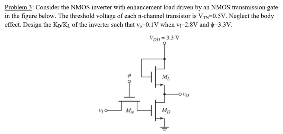
Problem 3: Consider the NMOS inverter with enhancement load driven by an NMOS transmission gate in the figure below. The threshold voltage of each n-channel transistor is VTN = 0.5 V. Neglect the body effect. Design the KD/KL of the inverter such that vo = 0.1 V when vI = 2.8 V and ϕ = 3.3 V.
